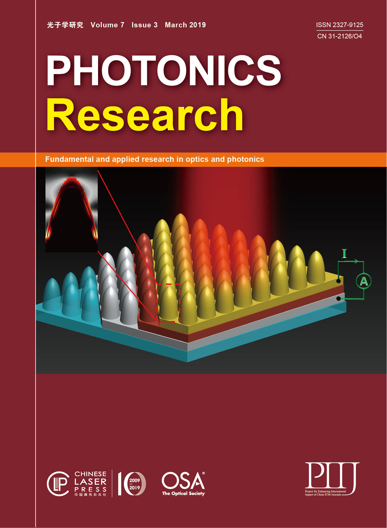
Photonics Research, 2019, 7 (3): 03000359, Published Online: Mar. 7, 2019   

Ultra-compact on-chip metaline-based 1.3/1.6  μm wavelength demultiplexer

Author Affiliations
1 Centre de Nanosciences et de Nanotechnologies, CNRS, Université Paris-Sud, Université Paris-Saclay, C2N—Avenue de la Vauve, 91220 Palaiseau cedex, France
2 Université Paris Lumières, Univ Paris Nanterre, 92410 Ville d’Avray, France
Abstract
In this paper, we report an experimental demonstration of enabling technology exploiting resonant properties of plasmonic nanoparticles, for the realization of wavelength-sensitive ultra-minituarized (4 μm×4 μm) optical metadevices. To this end, the example of a 1.3/1.6 μm wavelength demultiplexer is considered. Its technological implementation is based on the integration of gold cut-wire-based metalines on the top of a silicon-on-insulator waveguide. The plasmonic metalines modify locally the effective index of the Si waveguide and thus allow for the implementation of wavelength-dependent optical pathways. The 1.3/1.6 μm wavelength separation with extinction ratio between two demultiplexers’ channels reaching up to 20 dB is experimentally demonstrated. The considered approach, which can be readily adapted to different types of material planar lightwave circuit platforms and nanoresonators, is suited for the implementation of a generic family of wavelength-sensitive guided-wave optical metadevices.

Yulong Fan, Xavier Le Roux, Anatole Lupu, André de Lustrac. Ultra-compact on-chip metaline-based 1.3/1.6  μm wavelength demultiplexer[J]. Photonics Research, 2019, 7(3): 03000359.

本文已被 1 篇论文引用
被引统计数据来源于中国光学期刊网
引用该论文: TXT   |   EndNote

相关论文

加载中...

关于本站 Cookie 的使用提示

中国光学期刊网使用基于 cookie 的技术来更好地为您提供各项服务,点击此处了解我们的隐私策略。 如您需继续使用本网站,请您授权我们使用本地 cookie 来保存部分信息。
全站搜索
您最值得信赖的光电行业旗舰网络服务平台!