光电子技术, 2020, 40 (1): 13, 网络出版: 2020-04-26
基于端面耦合的InP基激光器/硅光波导混合集成技术研究  下载: 1025次
Hybrid Integration of InP FP Laser / Silicon Optical Waveguide Based on Silicon Edge Coupler
InP基激光器 硅光波导 端面耦合 混合集成 InP-based laser silicon-based optical waveguide edge coupler hybrid integration
摘要
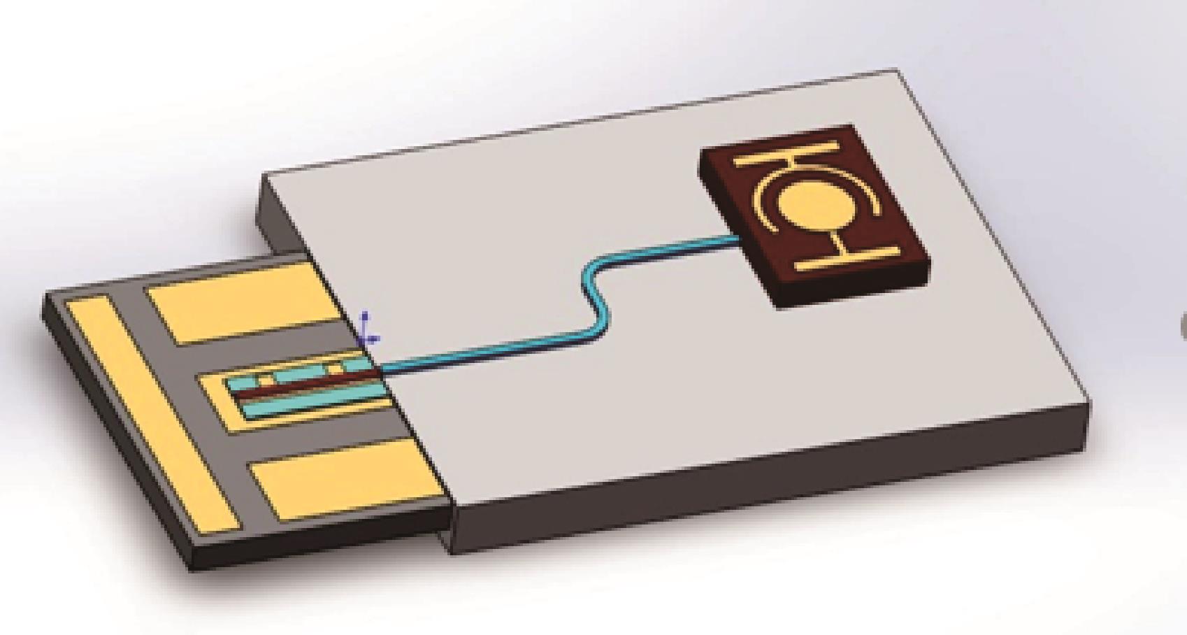
针对硅光子集成回路缺少实用化光源的问题,提出了一种1.55 μm波段InP基FP激光器芯片、InP基PIN光电探测器芯片与硅光波导芯片集成模块的设计与制备方法。使用CMOS工艺兼容的硅光无源器件制备工艺,设计并制备了倒拉锥型端面耦合器,与锥形透镜光纤耦合效率为36.7 %。采用微组装对准技术将激光器芯片与硅波导芯片耦合、UV固化胶固化后耦合效率为35.8 %,1 dB耦合对准容差横向为1.2 μm,纵向为0.95 μm。
Abstract
To solve the problem of practical light source lacking in silicon photonic integrated circuit, design and preparation method of integrated module including 1.55 μm InP FP laser chip, InP PIN photodetector chip and silicon optical waveguide was proposed. Silicon edge coupler of inverted cone type was fabricated by CMOS compatible process, and the coupling efficiency was 36.7 %. The laser chip and silicon waveguide chip were coupled by micro-assembly alignment technology, and the coupling efficiency was 35.8 % after UV adhesive curing. The 1 dB alignment tolerance was 1.2 μm horizontally and 0.95 μm longitudinally.
王艳, 王东辰, 徐鹏霄, 唐光华, 尤国庆, 孔月婵. 基于端面耦合的InP基激光器/硅光波导混合集成技术研究[J]. 光电子技术, 2020, 40(1): 13. Yan WANG, Dongchen WANG, Pengxiao XU, Guanghua TANG, Guoqing YOU, Yuechan KONG. Hybrid Integration of InP FP Laser / Silicon Optical Waveguide Based on Silicon Edge Coupler[J]. Optoelectronic Technology, 2020, 40(1): 13.


