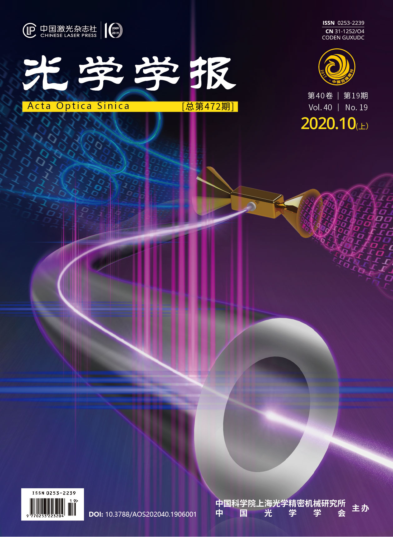
光学学报, 2020, 40 (19): 1914001, 网络出版: 2020-09-19
极低内部光学损耗975 nm半导体激光器  下载: 980次
975 nm Semiconductor Lasers with Ultra-Low Internal Optical Loss
摘要
通过对波导结构和P包层的掺杂分布进行优化,减少了光场与P包层掺杂区的交叠,从而减小了半导体激光器的内部光学损耗。同时使用宽带隙GaAsP作为势垒层可以减少有源区载流子泄露,实现了内部光学损耗为0.259 cm -1。所制备的975nm波长、100 μm条宽、4 mm腔长单管器件,在室温下器件的连续输出光功率达到21 W。当输出功率为20 W时,功率转换效率仍大于50%。
Abstract
By optimizing the doping distribution of the waveguide structure and the P-cladding layer, the overlap between the optical field and the P-cladding layer doped area is reduced, thereby reducing the internal optical loss of the semiconductor laser. At the same time, the use of wide band gap GaAsP as the barrier layer reduces the carrier leakage in the active region and achieves an internal optical loss of 0.259 cm -1. The prepared single emitter device with a wavelength of 975 nm, a stripe width of 100 μm and a cavity length of 4 mm has a continuous-wave output optical power of 21 W at room temperature. When the output power is 20 W, the power conversion efficiency is still greater than 50%.
曼玉选, 仲莉, 马骁宇, 刘素平. 极低内部光学损耗975 nm半导体激光器[J]. 光学学报, 2020, 40(19): 1914001. Yuxuan Man, Li Zhong, Xiaoyu Ma, Suping Liu. 975 nm Semiconductor Lasers with Ultra-Low Internal Optical Loss[J]. Acta Optica Sinica, 2020, 40(19): 1914001.


