Chinese Optics Letters, 2020, 18 (6): 063603, Published Online: Jun. 5, 2020  

High-Q factor photonic crystal cavities with cut air holes [Invited] Download: 809次

Author Affiliations
Key Laboratory of Space Applied Physics and Chemistry, Ministry of Education, and Shaanxi Key Laboratory of Optical Information Technology, School of Physical Science and Technology, Northwestern Polytechnical University, Xi’an 710129, China
Abstract
Planar photonic crystal (PPC) cavities with high quality (Q) factors were currently designed by missing or moving air holes. Here, we propose that cutting air holes in PPC into semicircles could be considered as another strategy to realize and optimize cavities, presenting superiorities over cavities with missed or moved air holes in a higher Q factor and a smaller mode volume (Vmode). Examples are demonstrated: (1) in a PPC lattice, cutting two adjacent air holes promises a cavity mode with a Q exceeding 200,500 and an ultrasmall mode volume Vmode < 0.329(λ/2 n)3; (2) in a PPC waveguide, cutting two air holes on opposite sides of the waveguide supports a cavity mode with a Q exceeding 104,600 and a Vmode < 1.22(λ/2 n)3; (3) cutting the two air holes at the edges of an L3-type PPC cavity, the Q factor is optimized from 5500 to 124,700, with an almost constant Vmode. The concept of cutting air holes to introduce defects in PPC also promises the design of PPC also waveguides with an engineered transmission loss and dispersion.

Planar photonic crystal (PPC) cavities fabricated in dielectric slabs have a variety of advantages to resonantly control light-matter interactions and light wave propagation[15" target="_self" style="display: inline;">5]. First, compared with other optical cavities, PPC cavities could be straightforwardly fabricated using the standard technologies developed for semiconductor electronic devices[6], facilitating their practical applications. Second, it is easy to construct photonic integrated circuits using PPC cavities, with the combination of other defect modes in the PPC structures, such as PPC waveguides[7]. The circuits are ultracompact and PPC cavities function as filters, memories, and switches[810" target="_self" style="display: inline;">–10]. PPC’s planar structures also allow the integration of electrical devices for optoelectronic circuits[11]. Third, PPC cavities are well recognized as one of the optical cavities with the highest Q/Vmode factor[12], where the Q and Vmode are the quality factor and mode volume of the resonant mode, respectively. The density of the electric field of a resonant mode is proportional to the Q/Vmode factor, which therefore enables PPC cavities as a promising platform to control light-matter interactions for highly efficient all-optical processes, nonlinear optics, optomechanics, and classical and quantum light emissions[10,1318" target="_self" style="display: inline;">18].

In the past decades, a number of designs have been reported to realize PPC nanocavities with a high Q factor and small Vmode[1923" target="_self" style="display: inline;">23]. PPCs are normally periodic air holes arranged with a two-dimensional triangular lattice, which support large photonic bandgaps for transverse electrical (TE) electromagnetic modes. If structure defects are involved into the PPC lattice, defect modes could originate inside the PPC’s photonic bandgap, giving rise to a PPC cavity. Summarized from the previously reported PPC cavities[1923" target="_self" style="display: inline;">23], missing air holes and moving air holes in PPCs are two of the most widely accepted defect designs, including the popular types of L3[19], H0[20], heterostructure[23], local width modulation[21], etc. These PPC cavities have virtues of simple design, high Q factor, small Vmode, and compact footprint.

Here, we propose that cutting two air holes in the PPC into semicircles is another important concept for realizing and optimizing cavities, which shows advantages over the cavities designed with missed or moved air holes in a higher Q factor and smaller Vmode. As examples, we present the formations of decent cavities by simply cutting two air holes either in a PPC lattice or in a PPC waveguide, as well as the great optimization of the typical L3-type PPC cavity by cutting two air holes at the cavity edges without movement of air holes.

Cavity formed by cutting air holes in PPC lattice - We first discuss the formation of a cavity by cutting a couple of air holes in a PPC lattice with periodic air holes, without missing or moving air holes. The PPC lattice is schematically displayed in Fig. 1(a), which is also employed to discuss other PPC cavities in this work. A silicon slab is chosen with a thickness of t=220nm and a refractive index of 3.48. The triangular lattice of air holes has a period of a=450nm and an air hole radius of r=0.26a. Figure 1(b) shows the structure of the proposed PPC cavity with cut air holes. Two adjacent air holes along the Γ-M direction in the center of the PPC lattice are cut into semicircles with D shapes, which have the same width of D. In contrast to the surrounding air holes with periodicity, the two semicircles have an increased effective dielectric permittivity between them that would support electromagnetic modes with optical frequencies locating inside the PPC’s photonic bandgap. Resonant modes are therefore formed with the confinement from the surrounding air holes, though there is no missed or moved air holes. To facilitate further discussions, we name the cavity arisen from cutting air holes in a PPC lattice as a D-type PPC cavity.
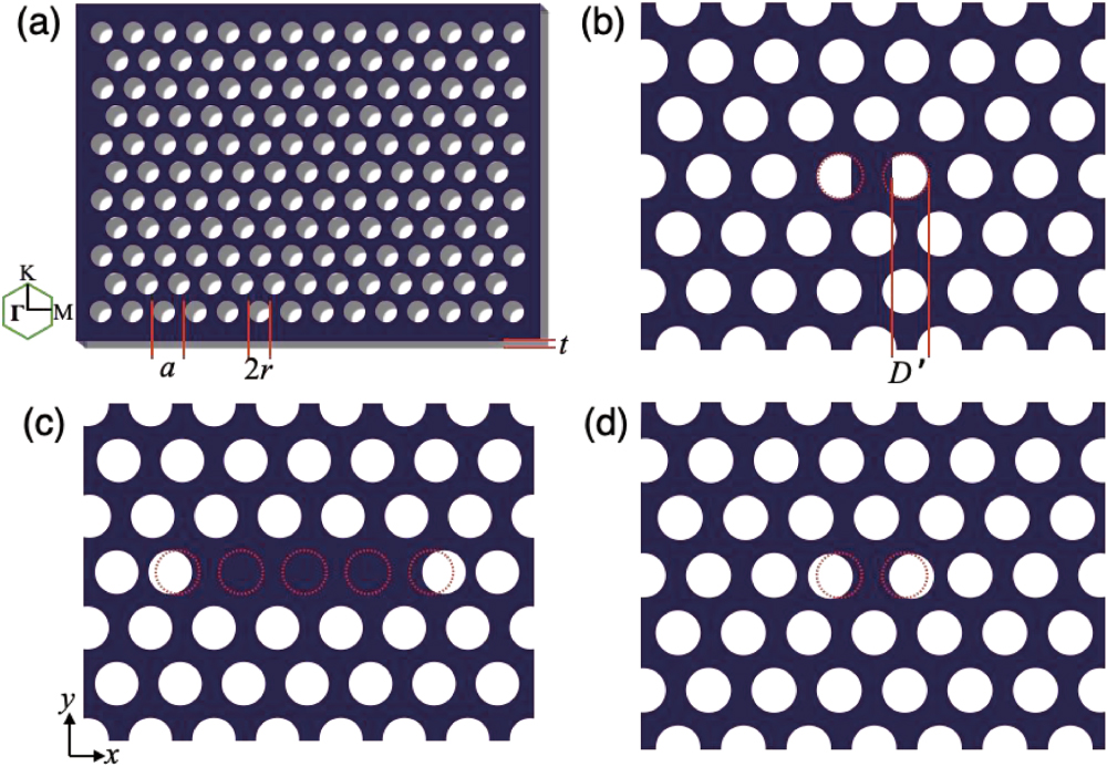
Fig. 1. (a) Schematic of the employed PPC lattice with a triangular lattice of air holes in a silicon slab. Inset: the reciprocal lattice of the PPC lattice. (b)–(d) Zoomed structures around the defect regions of the (b) D-, (c) L3-, and (d) H0-type PPC cavities. The initial positions and profiles of the air holes in the PPC lattice are denoted by dashed red circles.

下载图片 查看所有图片

To assess the resonant performances of the D-type PPC cavity, we also consider the resonant modes in widely studied L3- and H0-type PPC cavities with the same air hole lattice, whose structures are shown in Figs. 1(c) and 1(d), respectively. In the L3-type PPC cavity, the defect is formed by missing three air holes along the Γ-M direction in a PPC lattice[19]. To improve the Q factor, the two air holes next to the defect edge are moved outward to obtain gentle mode confinements[19]. The H0-type PPC cavity has no missed air holes, and the defect is formed by moving two adjacent air holes outward along the Γ-M direction in a PPC lattice[20]. For a PPC cavity, two of the most important figures of merit are Q factor and Vmode, which determine the performances of the Purcell factor with the Q/Vmode, strong-coupling cavity quantum electrodynamics with the Q/Vmode, and nonlinear optical responses with the Q2/Vmode[3]. Hence, the Q factor and Vmode of the resonant modes in these PPC cavities are calculated using the finite element method (COMSOL Multiphysics). For the L3-type PPC cavities with varied displacements of the two air holes at the defect edge, the highest Q factor of the fundamental resonant mode is obtained from a cavity with the displacement of 0.2a, which is 95,300. This fundamental resonant mode locates at the wavelength of 1669.5 nm, and the corresponding Vmode is 0.674(λ/2n)3, where λ and n are the resonant wavelength and refractive index of the silicon slab, respectively. In the H0-type cavity, by moving both air holes outward to a distance of 0.15a, the optimized fundamental mode has the highest Q factor of 107,600 and a Vmode=0.496(λ/2n)3 at the wavelength of 1514.1 nm.

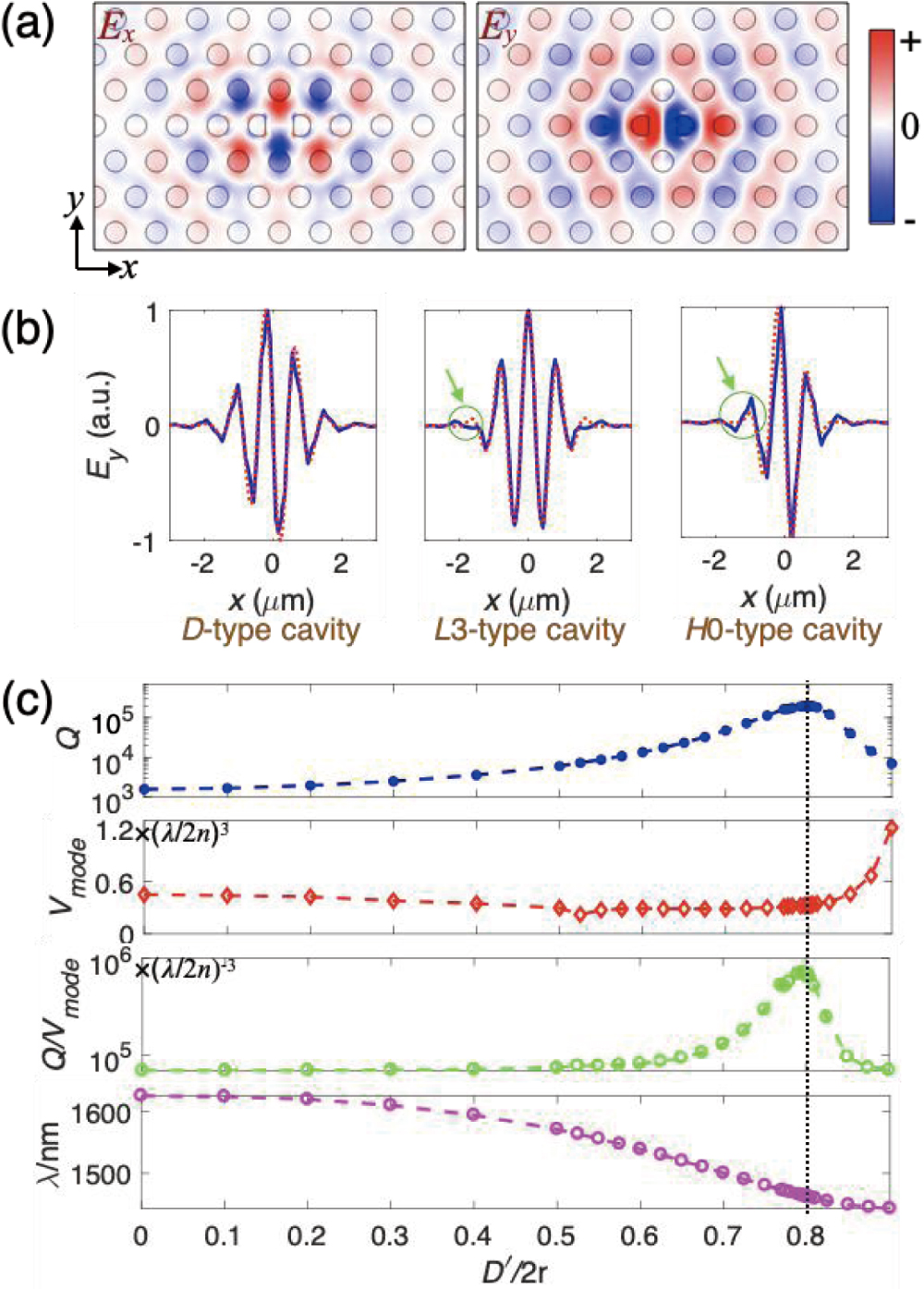
Resonant modes of D-type PPC cavities with different D(0<D<2r) are then studied. The highest Q factor of the fundamental resonant mode is obtained from the cavity with D=1.6r. This resonant mode locates at the wavelength of 1461.9 nm and has a Q factor of 200,500 and a Vmode=0.329(λ/2n)3. Compared with the optimized L3- and H0-type cavities mentioned above, the optimized D-type cavity has the highest Q factor and the smallest Vmode. Figure 2(a) displays the distributions of electric fields (Ex and Ey) of the optimized resonant mode. The two semicircles break the periodicity of the PPC lattice, and a strongly confined mode localizes between them. Since the physical length of the cavity defect formed by the two semicircles is much smaller than the mode wavelength, there are electromagnetic fields penetrating into the region outside the semicircles. It also accounts for the small Vmode. Both Ex and Ey present odd-symmetric distributions with respect to the defect center, indicating that their vertical far-field radiation will have oblique directions. While the mode strongly penetrates into the semicircles, the Q factor is still very high, which could be attributed to the relaxation of the impedance mismatch at the abrupt interfaces between air holes and the silicon slab with the assistance of cut air holes, which provides gentle mode confinements.

Fig. 2. (a) Electric field distributions (Ex and Ey) of the fundamental resonant mode in a D-type cavity with D=1.6r. (b) The Ey profiles of the resonant modes in D-, L3-, and H0-type cavities over the cavity centerline along the x direction (solid lines) and fitted curves calculated from the product of a Gaussian envelope function and a sinusoidal wave (dashed lines). (c) The Q factor, Vmode, Q/Vmode, and resonant wavelength of the fundamental resonant modes calculated from the D-type cavities with a varied D.

下载图片 查看所有图片

The main factor degrading Q factors in PPC cavities is the vertical radiation loss because the total internal reflection of the slab could not be satisfied for the light components with small in-plane wave vectors (in the range between 0 and 2π/λ0, where λ0 is the wavelength of light in air). In the L3- and H0-type cavities, to improve the Q factors, moving air holes near the cavity edge is required, which extends the cavity’s physical length to make the mode have more components with large in-plane wave vectors. However, as shown in Figs. 1(c) and 1(d), these air holes at the cavity edges are circularly shaped, which results in the abruptest variations of the dielectric impedance along the centerline of the cavity in the x direction. Unfortunately, the mode has the strongest electromagnetic field over this centerline. This contradiction makes it unfavorable to improve the Q factors, even with the outward shifts of air holes. In the proposed D-type cavity, the flat sides of the semicircles provide uniform variations of the dielectric impedance along the y direction. It is therefore beneficial to redirect more components of the mode to have large in-plane wave vectors and improve the Q factors. The electric field profiles shown in Fig. 2(a) reveal the flat mode distributions at the interfaces between air holes and the silicon slab, resulting in mode envelopes more similar to Gaussian functions in two dimensions. In the L3- and H0-type cavities, electric fields of the resonant modes are extruded away from the Gaussian envelopes by the circular air holes.

To illustrate this, we fit the fundamental resonant modes of the optimized D-, L3-, and H0-type cavities with curves corresponding to the products of a sinusoidal wave and a Gaussian function[24], as shown in Fig. 2(b). Here, the Ey components of these three resonant modes at the cavity centerline along the x direction are chosen. For each fitting, the blue solid line and red dashed line indicate the extracted electric field profile of the resonant mode and an ideal profile of the product of a sinusoidal wave and a Gaussian function, respectively. The sinusoidal wave has a period the same as that of the mode’s Ey profile. For the fitting results of the D-, L3-, and H0-type cavities, the electric fields match closely with the fitting curves in the central main lobes for the three cases. However, for the lobes at the cavity edges of the L3- and H0-type cavities, there are obvious discrepancies between the electric field profiles and the fitting curves, as indicated by the green circles in Fig. 2(b). In contrast, the mode in the D-type cavity could be fitted well even at the edge region. As demonstrated in Ref. [24], the Gaussian function is spatially localized without high-frequency wave vector components, and its envelope function could avoid abrupt changes at the cavity edge, which therefore guarantees that the resonant mode in the D-type cavity has higher Q factors than those in cavities formed by missing or moving air holes.

Note, for these D-, L3-, and H0-type PPC cavities, modifying air holes in the outer layers around the defects could improve the Q factor further by another one order of magnitude[2529" target="_self" style="display: inline;">29]. Considering that the main aim of this work is demonstrating the concept of cutting air holes for forming cavity modes in PPCs, further comparisons between these cavities by modifying air holes in outer layers will not be discussed here. We also carry out calculations of the three types of PPC cavities with other parameters of r/a, which show that the D-type cavity could achieve a higher Q factor and smaller Vmode than the other two types of cavities. Note, while the above optimized cavities are designed at specific wavelengths, resonance modes with maximum Q factors at other desired wavelengths could also be realized by changing the structure parameters of a, r/a, and t/a. In addition, with the above explanations and strategies, cutting the air holes into indented shapes to relax the impedance mismatch at the cavity edges could further improve the cavity Q factor, which will be discussed elsewhere.

We also study the dependences of the Q factor, Vmode, Q/Vmode, and resonant wavelength of the fundamental resonant mode on D in the D-type cavities, as shown in Fig. 2(c). While the maximum Q factor is obtained from the cavity with D=1.6r, the Q factors could be larger than 105 for the cavities with D in the range between 1.53r and 1.67r. Considering the employed a=450nm and air hole radius of r=0.26a, cavities with high Q factors could be realized when the semicircles have a width between 179 nm and 195 nm. This error tolerance could be satisfied by the mature fabrication techniques of silicon nanophotonic devices, which has fabrication imperfections less than 10 nm. This promises the feasibility of future fabrications of the proposed D-type PPC cavity. For the cavities with D>1.6r, the Q factor of the fundamental resonant mode decreases as D becomes larger. While it is possible to form an electromagnetic mode with the optical frequency locating inside the photonic bandgap of the PPC lattice by cutting the two air holes, to support the standing wave of a resonant mode in the cavity defect with an ultrasmall physical length, it should have a small in-plane wave vector[28,30]. The corresponding vertical wave vector is consequently large, which tends to shift the electromagnetic mode toward the region of the slab’s light core and break the vertical total internal reflection of the silicon slab. Hence, when D becomes larger, the length of the cavity defect shrinks, resulting in severe mode scattering and Q factor degrading. For the case of D>1.8r, it is difficult to find a fundamental resonant mode due to the non-convergence in the mode simulation, indicating that the mode shifts into the light core already. In addition, because of the small in-plane wave vector in the cavity with a large D, the resonant mode penetrates into the outer layers of the air holes remarkably, giving rise to a large Vmode. As shown in Fig. 2(c), the Vmode of the resonant mode in the cavity with D=1.8r is 1.220(λ/2n)3, which is almost three times that in the optimized cavity.

For the cavities with D<1.6r, the Q factor of the fundamental resonant mode decreases gradually as D is reduced from 1.6r and reaches the smallest value for D=0. Compared with the cavities with D>1.6r, the physical lengths of the cavity defects in these cavities with a narrower D are much larger, and the in-plane wave vectors of the modes are large enough to ensure them being away from the light cone. However, the narrower width of D causes the mode distribution to have smaller values outside the cavity edge (x=2.5a) than that required for a standard Gaussian envelope, which causes strong mode scattering from the air holes outside the cavity edge. Note, in the case of D=0, the D-type cavity evolves into a cavity with two missed air holes, i.e., the L2-type cavity. The Q factor is as low as 1500 because the mode profile strongly deviates from the ideal Gaussian envelope, which is the same mechanism for the low Q factor in the standard L3-type cavity without moved air holes[31]. In addition, compared with the optimized D-type cavity, the cavity with a smaller D has a larger physical dimension, which results in a larger Vmode. In the cavity with D=0, the Vmode is about 0.450(λ/2n)3. For the D-type cavities with a different D, the factor of Q/Vmode has the similar trend to that of the Q factor due to the small variation of the Vmode. It indicates that the optimized cavity for the maximum Q factor also supports the highest Q/Vmode factor for enhancing light-matter interactions. However, the resonant wavelengths of the fundamental modes vary strongly, as shown Fig. 2(c). There is a monotonic decreasing function between the resonant wavelength and D. Resonant modes in PPC cavities are standing waves. In a cavity with a narrower D, the larger physical length of the cavity defect allows a longer resonant wavelength to form a constructive interference.

In the previously reported PPC cavities, such as L3- and H0-type cavities, besides the fundamental resonant mode, it is also possible to form higher-order resonant modes with higher optical frequencies, though the Q factors are normally smaller than that of the fundamental resonant mode due to the smaller in-plane wave vectors[30]. In realistic applications of PPC cavities, this multi-mode behavior is not preferred. For instance, in micro-lasers based on PPC cavities, the multiple resonant modes would compete for the gain and subsequently increase the laser threshold, which also hinders the single-mode operation of the laser. To employ PPC cavities in optical sensors, the multiple modes limit the sensing range when the shift of resonant wavelength is utilized to monitor the parametric variations. As discussed above, because the physical length of the defect in the D-type cavity is very small, especially for the case with a large D, the in-plane wave vector of the fundamental resonant mode is very small. For the higher-order electromagnetic mode supported by the cavity defect, which has even smaller in-plane wave vectors and higher optical frequencies, it is difficult for it to form a resonant mode with a moderately high Q factor. Because the modes are even closer to the light cone in the energy-momentum space, hence, it is expected that the ultracompact D-type cavity has the single-mode operation. From our calculations, for the cavity with D=1.6r, which is optimized for the fundamental resonant mode, the higher-order resonant mode cannot be convergent in the mode simulation. This single-mode property enables the D-type cavity to have potentials in the single-mode lasing, large range optical sensing, and deterministic single photon sources. Of course, by narrowing the D to allow a longer cavity length, a higher-order resonant mode would be present. For example, in a cavity with D=0.8r, a higher-order resonant mode with a Q factor of 1800 and a Vmode of 0.353(λ/2n)3 is obtained at the wavelength of 1452.3 nm. Note that it is more than 140 nm away from the fundamental resonant mode (at the wavelength of 1594.2 nm), which could guarantee the single-mode operation in a large wavelength range.

Inducing a cavity in PPC waveguide with cut air holes - A PPC waveguide, with a line defect of missed air holes, is another important base structure for realizing PPC cavities that represent advantages over the cavities directly designed from the PPC lattice. To generate a cavity from the PPC waveguide, modifications of a section of the waveguide are normally exploited to induce a varied effective refractive index, which forms mode gap regions in the photonic band. Consequently, cavity modes are created below the transmission band of the PPC waveguide. In the cavities derived from the PPC waveguide, along the direction of the line defect in the waveguide, the resonant mode confinements are much gentler due to the absence of air holes, which is different from the cavity based on a PPC lattice. This makes the electric-field profile of the cavity mode close to the ideal Gaussian curve, promising high Q factors[24]. In addition, inducing a cavity based on a PPC waveguide could facilitate the coupling of the resonant modes directly. For the cavity originated from a PPC lattice, an extra side coupled PPC waveguide is normally required to access the resonant modes[32].

The previously reported modifications of PPC waveguides for generating cavities include setting different horizontal lattice constants over a few periods to form a heterostructure[23] and outward moving air holes adjacent to the line defect of the waveguide to locally tune the waveguide width[21]. Here, we illustrate that simply cutting two air holes on opposite sides of the PPC waveguide’s line defect could form a PPC cavity with high Q resonant modes. The structure is schematically shown in Fig. 3(a). By setting the width of the semicircle as D=1.6r, a resonant mode with a Q factor of 104,600 and Vmode=1.352(λ/2n)3 is obtained at the wavelength of 1688.8 nm. The larger Vmode and longer resonant wavelength compared with those in the above discussed D-type PPC cavity are due to the longer physical length of the defect region in this waveguide-based cavity, as indicated by the simulated mode distributions displayed in Fig. 3(b). Both Ex and Ey fields have odd symmetry with respect to the center of the defect region formed by the two semicircles, which implies that this resonant mode derives from the odd transmission band of the standard PPC waveguide. In addition, while the cavity defect is between the two semicircles, the mode distribution extends along the x direction by couple wavelengths, which could guarantee the gentle impedance mismatch and the high Q factor.
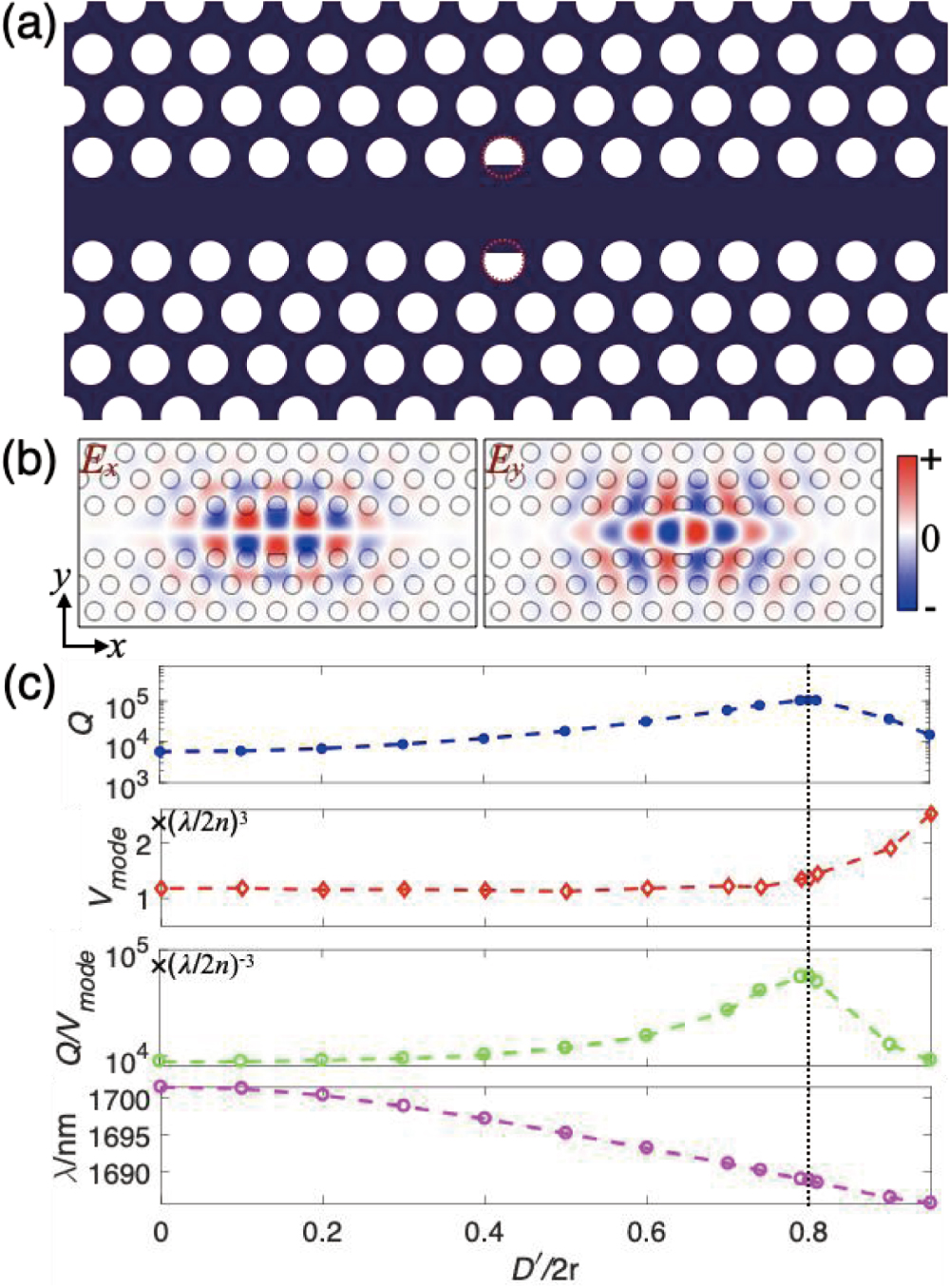
Fig. 3. (a) Schematic structure of the cavity induced by cutting two air holes adjacent to the line defect of a PPC waveguide. The dashed red circles represent the initial profiles of the cut air holes. (b) The electric field distributions (Ex and Ey) of the fundamental resonant mode with D=1.6r. (c) The Q factor, Vmode, Q/Vmode, and resonant wavelength of the fundamental resonant modes versus D.

下载图片 查看所有图片

Instead of cutting the two air holes, the cavity induced by outward moving the two air holes away from the line defect of the PPC waveguide is studied as well for comparison. The resonant mode with the highest Q factor is obtained from a cavity with a displacement of 0.07a, and the Q factor is 96,700, which is smaller than that obtained from the cavity with cut air holes. This could also be explained by the flat interface of the semicircles facing the mode distributions, which more relaxes the scattering loss induced by the impedance mismatch. In addition, we also consider the PPC cavity formed by cutting more air holes adjacent to the PPC waveguide defect. Even higher Q factors are obtained than that with two cut air holes due to the wider mode distribution, while the Vmode becomes larger.

Figure 3(c) plots the Q factor, Vmode, Q/Vmode, and resonant wavelength of the fundamental resonant modes calculated from the cavity by cutting the air holes into different values of D in the PPC waveguide. The variation trends of these figures of merit are similar to those obtained in the D-type cavities. For the cavities with D>1.6r, with the reduced Q factor, the Vmode increases significantly due to the bad confinement of the mode. In these cavities, because the cavity defect is too small, the resonant mode extends strongly along the waveguide direction (x direction) governed by the small in-plane wave vector. For the cavities with D<1.6r, while the Q factors are degraded as well, the Vmode is almost constant. This could be attributed to the well-confined mode tails along the waveguide direction due to the moderately large cavity defect. However, with the large cut air hole, the mode profiles deviate from the ideal Gaussian envelope around the cavity edge, which causes more mode scatterings. The factor of Q/Vmode has a similar trend to that of the Q factor. The resonant wavelengths exhibit a monotonic decreasing function versus D considering larger cavity dimensions for a smaller D.

Optimizing L3 PPC cavity with cut air holes - We further demonstrate that the strategy of cutting air holes could also be employed to optimize the Q factor of the widely studied Lm-type PPC cavity, where m is the number of missed air holes in the defect region. In an Lm-type PPC cavity, to improve Q factors, outward moving the nearest-neighbor air holes at the cavity edge is essential to make the electric field profile vary more gently, as shown in Fig. 1(c) for the L3-type PPC cavity. As discussed above, the origin of high Q factors in D-type PPC cavities is that the cut air holes have flat sides to improve the impedance match between the air holes and the silicon slab compared to the circular air holes. Therefore, it is also possible to optimize the Q factor in the Lm-type PPC cavity by cutting the two air holes at the cavity edge to relax the abrupt change of mode fields. Taking the L3-type PPC cavity as an example, the optimized structure is schematically displayed in Fig. 4(a). The two air holes at the defect edge are cut into semicircles without any position tuning.
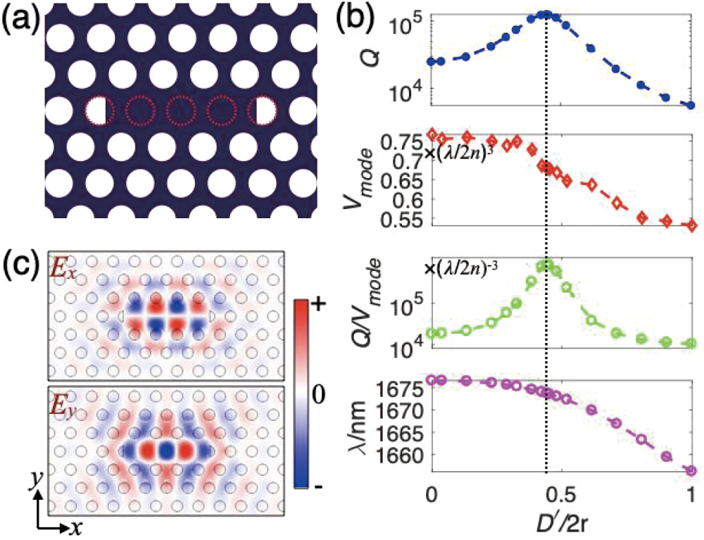
Fig. 4. (a) Schematic structure of the L3-type cavity with cut air holes at the cavity edge. The dashed red circles represent initial positions and profiles of the air holes in the PPC lattice. (b) The electric field distributions (Ex and Ey) of the fundamental resonant mode with D=0.9r. (c) The Q factor, Vmode, Q/Vmode, and resonant wavelength of the fundamental resonant mode versus D.

下载图片 查看所有图片

Figure 4(b) displays the Q factor, Vmode, Q/Vmode, and resonant wavelength of the fundamental resonant mode in the modified L3-type cavity versus D. When the D is reduced from 2r to 0, both the resonant wavelength and Vmode increase gradually because of the lengthened physical length of the cavity. However, the Q and Q/Vmode factors achieve their maximum values. For the standard L3-type cavity without any air hole moving and cutting (D=2r), the fundamental resonant mode at the wavelength of 1656.2 nm has a Q factor of 5500 and a Vmode of 0.531(λ/2n)3. As the two-circular air holes at the cavity edge are cut into semicircles, the Q factor increases gradually and reaches the maximum of 124,700 for the case of D=0.9r, i.e., the Q factor is improved by more than 20 times compared with the standard L3-type cavity. The corresponding Vmode of the optimized resonant mode is 0.679(λ/2n)3, which is lightly enlarged from that of the standard L3-type cavity. In the optimized L3-type cavity by moving the two edge air holes, as discussed above, the fundamental resonant mode has a Q factor of 95,300, a Vmode of 0.674(λ/2n)3, and a central wavelength of 1669.5 nm. Compared to the optimized L3-type cavities with cut air holes and moved air holes, the Vmode and resonant wavelength of the fundamental resonant mode are very close. However, the Q factor in the optimized cavity with cut air holes is higher. This could be explained by more relaxation of impedance mismatch at the boundary of air holes and the silicon slab with the flat side of the semicircles. Figure 4(c) displays the electric field distributions (Ex and Ey) of the fundamental resonant mode, showing the similar mode distributions to that in the standard L3-type cavities or cavities with moved air holes.

By further cutting the two air holes with D<0.9r, the Q factor decreases gradually. This could be attributed to the deviation of the mode profile over the cavity centerline from the ideal Gaussian envelope function, similar to that discussed for the D-type cavity. An abrupt change of the mode profile still remains at the cavity edge. For the case with D=0, the Q factor decreases to a relatively small value of 24,900. Note that it is still higher than that in the standard L3-type cavity. It could be understood that the L3-type cavity with D=0 evolves into a standard L5-type cavity, which has larger in-plane wave vector benefitting from the longer physical defect length[30]. Hence, the vertical scattering for the resonant mode in the L5-type cavity should be smaller than that in the L3-type cavity, promising a higher Q factor.

In conclusion, we have demonstrated that simply cutting air holes in PPC to semicircles could be considered as a new strategy to form and optimize PPC cavities. Three examples are described. In the formations of PPC cavities, by simply cutting two adjacent air holes in a PPC lattice or two air holes on the opposite sides of a PPC waveguide, resonant modes with a Q factor exceeding 105 are obtained. In the optimization of the PPC cavity, by cutting the two air holes at the edge of an L3-type cavity, the Q factor is optimized by more than 20 times, while Vmode is almost constant. Results of these three examples also indicate that the cavities with cut air holes have superiorities over cavities with missed or moved air holes in the higher Q factor and smaller Vmode. In the cavities with missed or moved air holes, the air holes around the cavity edges are circularly shaped. By contrast, the cut air holes have flat sides facing the strong mode distribution, which could relax the impedance mismatch at the interfaces of air holes and the silicon slab more. Hence, cut air holes could enable much gentler mode confinement in PPC cavities. The cut air hole as a structure parameter provides a new strategy to design other PPC devices, such as PPC waveguides with engineered dispersions and low transmission losses.

References

[1] NotomiM., Rep. Prog. Phys.73, 096501 (2010).

[2] LiM.LiangH.LuoR.HeY.LinQ., Laser Photonics Rev.13, 1800228 (2019).

[3] VuckovicJ.EnglundD.FattalD.WaksE.YamamotoY., Phys. E32, 466 (2006).

[4] BurresiM.KampfrathT.Van OostenD.PrangsmaJ. C.SongB. S.NodaS.KuipersL., Phys. Rev. Lett.105, 123901 (2010).PRLTAO0031-9007

[5] SongB.-S.AsanoT.JeonS.KimH.ChenC.KangD. D.NodaS., Optica6, 991 (2019).

[6] AshidaK.OkanoM.OhtsukaM.SekiM.YokoyamaN.KoshinoK.MoriM.AsanoT.NodaS.TakahashiY., Opt. Express25, 18165 (2017).OPEXFF1094-4087

[7] EnglundD.FaraonA.ZhangB.YamamotoY.VučkovićJ., Opt. Express15, 5550 (2007).OPEXFF1094-4087

[8] TanabeT.NotomiM.MitsugiS.ShinyaA.KuramochiE., Appl. Phys. Lett.87, 151112 (2005).APPLAB0003-6951

[9] NozakiK.ShinyaA.MatsuoS.SuzakiY.SegawaT.SatoT.KawaguchiY.TakahashiR.NotomiM., Nat. Photonics6, 248 (2012).NPAHBY1749-4885

[10] KuramochiE.MatsudaN.NozakiK.ParkA. H. K.TakesueH.NotomiM., Opt. Express26, 9552 (2018).OPEXFF1094-4087

[11] NozakiK.MatsuoS.FujiiT.TakedaK.OnoM.ShakoorA.KuramochiE.NotomiM., Optica3, 483 (2016).

[12] AsanoT.OchiY.TakahashiY.KishimotoK.NodaS., Opt. Express25, 1769 (2017).OPEXFF1094-4087

[13] RivoireK.LinZ.HatamiF.VučkovićJ., Appl. Phys. Lett.97, 043103 (2010).APPLAB0003-6951

[14] GavartinE.BraiveR.SagnesI.ArcizetO.BeveratosA.KippenbergT. J.Robert-PhilipI., Phys. Rev. Lett.106, 203902 (2011).PRLTAO0031-9007

[15] GanX.MakK. F.GaoY.YouY.HatamiF.HoneJ.HeinzT. F.EnglundD., Nano Lett.12, 5626 (2012).NALEFD1530-6984

[16] GanX.GaoY.Fai MakK.YaoX.ShiueR. J.Van Der ZandeA.TrusheimM. E.HatamiF.HeinzT. F.HoneJ.EnglundD., Appl. Phys. Lett.103, 181119 (2013).APPLAB0003-6951

[17] NozakiK.ShinyaA.MatsuoS.SatoT.KuramochiE.NotomiM., Opt. Express21, 11877 (2013).OPEXFF1094-4087

[18] SunS.KimH.SolomonG. S.WaksE., Nat. Nanotechnol.11, 539 (2016).NNAABX1748-3387

[19] AkahaneY.AsanoT.SongB. S.NodaS., Nature425, 944 (2003).

[20] ZhangZ.QiuM., Opt. Express12, 3988 (2004).OPEXFF1094-4087

[21] KuramochiE.NotomiM.MitsugiS.ShinyaA.TanabeT.WatanabeT., Appl. Phys. Lett.88, 041112 (2006).APPLAB0003-6951

[22] RyuH. Y.NotomiM.LeeY. H., Appl. Phys. Lett.83, 4294 (2003).APPLAB0003-6951

[23] SongB. S.NodaS.AsanoT.AkahaneY., Nat. Mater.4, 207 (2005).NMAACR1476-1122

[24] TanakaY.AsanoT.NodaS., J. Lightwave Technol.26, 1532 (2008).JLTEDG0733-8724

[25] KuramochiE.GrossmanE.NozakiK.TakedaK.ShinyaA.TaniyamaH.NotomiM., Opt. Lett.39, 5780 (2014).OPLEDP0146-9592

[26] DharanipathyU. P.MinkovM.ToninM.SavonaV.HoudréR., Appl. Phys. Lett.105, 101101 (2014).

[27] LaiY.PirottaS.UrbinatiG.GeraceD.MinkovM.SavonaV.BadolatoA.GalliM., Appl. Phys. Lett.104, 241101 (2014).APPLAB0003-6951

[28] MaenoK.TakahashiY.NakamuraT.AsanoT.NodaS., Opt. Express25, 367 (2017).OPEXFF1094-4087

[29] MinkovM.SavonaV.GeraceD., Appl. Phys. Lett.111, 131104 (2017).

[30] OkanoM.YamadaT.SugisakaJ.YamamotoN.ItohM.SugayaT.KomoriK.MoriM., J. Opt.12, 075101 (2010).

[31] AkahaneY.AsanoT.SongB.-S.NodaS., Opt. Express13, 1202 (2005).OPEXFF1094-4087

[32] NotomiM.KuramochiE.TanabeT., Nat. Photonics2, 741 (2008).NPAHBY1749-4885

Liang Fang, Xuetao Gan, Jianlin Zhao. High-Q factor photonic crystal cavities with cut air holes [Invited][J]. Chinese Optics Letters, 2020, 18(6): 063603.

引用该论文: TXT   |   EndNote

相关论文

加载中...

关于本站 Cookie 的使用提示

中国光学期刊网使用基于 cookie 的技术来更好地为您提供各项服务,点击此处了解我们的隐私策略。 如您需继续使用本网站,请您授权我们使用本地 cookie 来保存部分信息。
全站搜索
您最值得信赖的光电行业旗舰网络服务平台!