Efficient second harmonic generation in silicon covered lithium niobate waveguides  Download: 630次
1. Introduction
Silicon on insulator (SOI) technology in the semiconductor industry has promoted the evolution and applications of compact photonic integrated devices in the past few decades[1]. Similarly, another promising optical platform referred to as lithium niobate on insulator (LNOI) has also sparked significant interest in exploring new optical phenomena and novel functionalities for integrated nanophotonic devices[2
To achieve efficient wavelength conversion in LNOI waveguides, phase matching among the interacting waves should be rigorously satisfied, relying on several schemes such as quasi-phase matching (QPM)[28
In this Letter, we theoretically propose an alternative method to achieve highly efficient SHG assisted with the hybrid Si-LN waveguide. For -cut LNOI, a hybrid waveguide for modal phase matching can be formed just by etching silicon on the top surface instead of the difficult reactive ion etching (RIE) of LN itself, alleviating the fabrication challenge. Due to the high refractive index of Si, it provides a fertile ground for multiple hybrid modes, and the generated hybrid modes are tightly but asymmetrically localized within the composite waveguide. By breaking the spatial symmetry of the waveguide, the fundamental mode of pumps can automatically phase match with a first-order mode of harmonic waves, leading to small mode area and large mode overlap for the nonlinear process. Though the Si inevitably introduces loss in the visible, the strong enhancement on the SHG efficiency is still clearly observed. Our proposal surely reveals the potential for wide applications in linear and nonlinear hybrid integration of Si and LN nanophotonics.
2. Theoretical Design
To demonstrate the design principle, we made an elaborate investigation in -cut LNOI, which has an LN layer with a thickness of 300 nm, underneath which is a 1.8-µm-thick substrate. Note that most efficient nonlinear optical processes have been performed in -cut LNOI wafers in consideration of the electric field poling technology for phase matching, whereas the wave is restricted to propagate only in the direction to utilize the largest nonlinear coefficient. In contrast, there is no such limitation in -cut LNOI wafers, since the wave can propagate in all directions in quasi-transverse-magnetic (TM) modes. The capability of maintaining phase matching on the entire x–y plane is benefitial for integrating arbitrarily guided structures like microrings and microdisks[39]. Therefore, we verify our design principle in -cut LNOI wafers. To construct a hybrid waveguide, Si is chosen as the ideal auxiliary material for a few reasons. First, Si has a pretty high refractive index compared with many other materials including LN, making it suitable for strong optical confinement and supporting more complex hybrid modes benefiting from flexible dispersion engineering. Second, the nanofabrication technology for Si is mature and has been well-developed for Si photonics. Third, Si also has a low optical absorption loss and has been demonstrated for high-quality devices at telecom wavelengths, though it has considerable loss at the visible wavelengths. Furthermore, the combination of Si and LN provides a highly desirable platform for emerging hybrid integrated devices and applications.
The schematic structure of the proposed -cut Si-LNOI hybrid waveguide for highly efficient SHG is shown in Fig. 1(a). A -cut LN thin film is located on the low index buffer layer, fabricated via ion-slicing and crystal bonding (available in NANOLN Company). An amorphous Si layer is chemically deposited on the top surface of the LN film and then etched to form a stripe. The LNOI film together with the Si stripe serves as a hybrid high-efficiency wavelength convertor. For simplicity, we consider the stripe has a rectangular cross section, which is achievable since the fabrication technology of Si is quite mature. As illustrated in Fig. 1(b), the geometric parameters of this LNOI etchless waveguide include LN height , Si height , and Si width . The coordinates in Figs. 1(a) and 1(b) are all aligned with the crystalline directions of LN, where is the extraordinary axis. Traditionally, monolithic waveguide supports simple guided modes, including both quasi-transverse-electric (TE) and quasi- TM modes. Note that conversion between the fundamental mode at the fundamental wavelength and first-order mode at the second harmonic (SH) wavelength is prohibited by symmetry (mode overlap of near zero); a common solution is to use higher-order modes for SH light but with a significant sacrifice of efficiency[37,39], whereas the situation in the hybrid waveguide becomes entirely different, especially for integration with high refractive index materials like Si. Due to mode coupling and hybridization, the mode symmetry is broken, which offers us an opportunity to take advantage of the large mode overlap provided by the first-order mode of SH light with the fundamental mode of the pump wave.
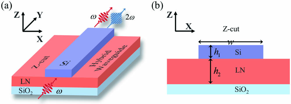
Fig. 1. Highly efficient SHG in modal phase-matched z-cut Si-LNOI hybrid waveguide. (a) Schematic and working principle of the Si-LN hybrid waveguide. (b) Cross-section schematic of the waveguide structure.
In order to access the largest nonlinear coefficient in the -cut waveguide, here we investigate the TM modes and engineer the geometric dispersion for phase matching by designing the height and width of the Si stripe. First, we demonstrate the effective refractive indices of the Si-LNOI hybrid waveguide as functions of the Si height both at pump wavelength (1550 nm) and SH wavelength (775 nm) in Fig. 2(a). The results are obtained by the finite difference eigenmode solver (MODE solutions, Lumerical), and other dimensions are set as and , considering the potential fabrication condition. In the simulation, the optical properties of the Si and LN are extracted from our experimental data and Palik database, respectively. The blue dotted lines illustrate part of the hybrid TE and TM modes at 775 nm, the blue curve shows the extraordinary hybrid mode at 775 nm, and the red curve shows the fundamental mode at 1550 nm. The discontinuities and crossing of the curves are exactly due to the mode hybridization. A detailed modal phase matching condition between at 775 nm and at 1550 nm is illustrated in Fig. 2(b), indicating a suitable Si height around 186.7 nm. From the dispersion relationship, it is not difficult to find that the mode phase matching condition is sensitive to the Si height, because the refractive index of Si is so large compared with the thin-film layer that it makes a significant difference to the mode indices when changing height. Afterwards, we also explore the relationship between the mode effective indices of the waveguide and the Si width at both wavelengths in Fig. 2(c) and the zoom-in Fig. 2(d), while other parameters are fixed at and . Numerical simulations demonstrate that at 1550 nm can be phase matched to at 775 nm with Si width . Apparently, the mode effective indices vary slowly with the change of the Si stripe width, revealing that achieving phase matching by changing the Si width is more robust than by changing the height. In other words, it is more practical to engineer the width of the Si in actual experiments. Representative phase-matched modal profiles of components at both wavelengths are displayed in Fig. 2(e), where the top two insets show the electric fields in all space, and the bottom two insets show the electric fields in the LN layer. Figure 2(f) shows the field as a function of the vertical position at the center of the waveguide, with the tangerine shaded area indicating the nonlinear LN material, and the purple area representing the Si material. Obviously, the loaded Si stripe in our scheme plays two important roles benefitting from its large refractive index. One is to confine the optical fields into a small scale, and the other is to break the spatial symmetry and hybridize the waveguide modes. Such hybrid modes are asymmetric and mainly localized in the nonlinear region, making a crucial contribution to the efficient SHG process. Though the electric field () of the 775 nm mode changes its polarity across the waveguide core, while that of the 1550 nm mode remains single, the polarity inside the nonlinear layer is single, leading to a very large net mode overlap. From this point, the nonlinear process in our design is analogous to SHG realized between two fundamental modes with large overlap in the LN layer. Detailed simulation results show that the overlap factor of such a hybrid waveguide is up to 0.9932, and the effective mode area is , calculated by the following expressions[38,40]:
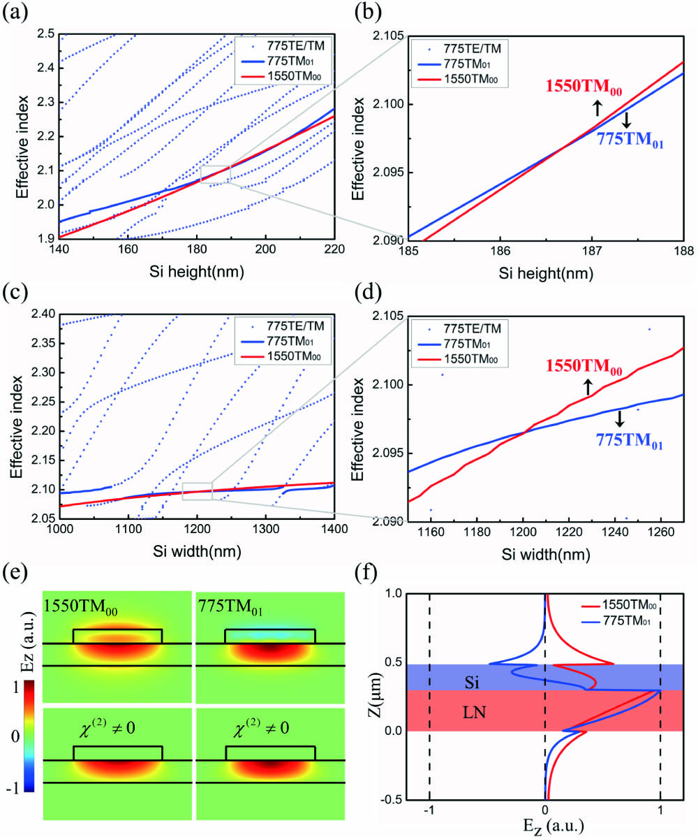
Fig. 2. Design of the LN etchless hybrid waveguide. Effective indices of the hybrid modes at both pump and SH wavelengths varying with (a) Si height and (c) Si width. (b), (d) Detailed phase matching conditions between TM01 at 775 nm and TM00 at 1550 nm of (a), (c). (e) Optical field (Ez components) of the phase-matched modes at both wavelengths in the all space and nonlinear region. (f) Ez as a function of the vertical position z at the center of the waveguide.
3. Calculation and Simulation
The typical characterization of nonlinear conversion for a lossless waveguide without pump depletion is the normalized efficiency (, where and correspond to SH and pump powers, and is the interaction length). Though the material induced loss in such a Si assisted hybrid waveguide is considerable, especially for the SH wave, here, we can still define the normalized efficiency to evaluate the performance of our device. The only difference that should be emphasized is that the normalized efficiency is no longer a constant but will decrease in propagation. Consequently, we analyze the dynamics of SHG based on the coupled-wave theory as
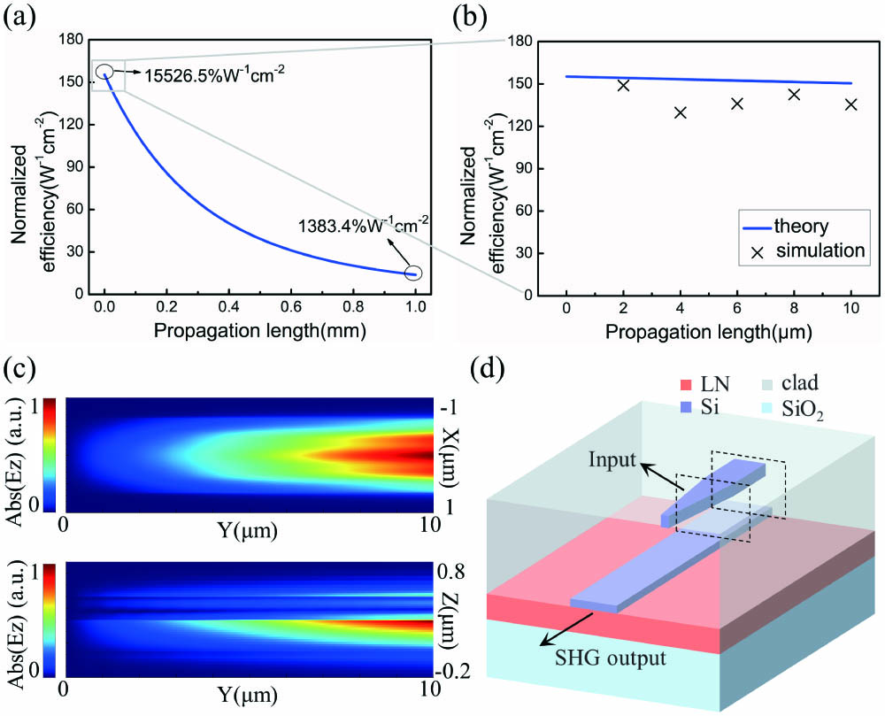
Fig. 3. Theoretical calculations and full-wave simulations. (a) Calculated normalized conversion efficiency as a function of the propagation length. (b) Simulation result in comparison with theory result. (c) Simulated SHG process in a 10-µm-long hybrid z-cut waveguide for demonstration. (d) Schematic of a fully integrated Si/LN hybrid system.
4. Discussion and Conclusion
In general, SHG in periodically poled waveguides is superior to that in modal dispersion phase-matched waveguides in efficiency, because the interaction waves in the former are both fundamental modes, while the SH wave in the latter usually is a higher-order mode, which severely undermines mode overlap with the pump wave. However, in consideration of the fabrication technology, the circumstances usually reverse. To tackle this conflict, our proposed Si-LN hybrid waveguide can maintain a high efficiency in the SHG process while simplifying the fabrication process. Within the fabrication capability, the amorphous Si can be deposited using plasma enhanced chemical vapor deposition (PECVD), followed by dry etching using RIE to form the stripe. It is worth noting that, although various materials can be employed for defining the stripe, Si is the optimal choice currently considering the high refractive index and compatibility to the Si photonics platform. In this regard, our strategy is suitable for ultrahigh-efficiency wavelength conversion within a short distance for on-chip integrated optical devices. For example, it would be possibly adopted for the telecom light conversion from the near-infrared (NIR) to short-wavelength SHG by vertical adiabatic waveguide couplers [e.g., see Fig. 3(d)], which would favor on-chip detection, modulation, and routing within LN photonic chips.
In conclusion, we have proposed a new design of an LNOI etch-free hybrid waveguide to address efficient on-chip SHG by integration of high refractive index material (Si) and -cut LNOI. The hybrid fundamental mode of the pump and asymmetric first-order mode of the SH wave are employed for modal phase matching with large mode overlap and small mode area, indicating a high normalized conversion efficiency. Particularly, such a prototype is talented for short-distance conversion with ultrahigh efficiency (more than for a 0.4-mm-long propagation distance). Another advantage of our design is that the fabrication process can be simplified by loading a Si stripe to construct the waveguide, overcoming the challenges in etching of LN material. Our approach might represent a new paradigm in hybrid integration of LN membranes onto Si photonic integrated circuits and reveals a roadmap towards future small footprint integrated nonlinear photonic devices.
[1] B. Jalali, S. Fathpour. Silicon photonics. J. Lightwave Technol., 2006, 24: 4600.
[2] P. Rabiei, J. Ma, S. Khan, J. Chiles, S. Fathpour. Heterogeneous lithium niobate photonics on silicon substrates. Opt. Express, 2013, 21: 25573.
[3] L. Chen, Q. Xu, M. G. Wood, R. M. Reano. Hybrid silicon and lithium niobate electro-optical ring modulator. Optica, 2014, 1: 112.
[4] A. Rao, A. Patil, J. Chiles, M. Malinowski, S. Novak, K. Richardson, P. Rabiei, S. Fathpour. Heterogeneous microring and Mach–Zehnder modulators based on lithium niobate and chalcogenide glasses on silicon. Opt. Express, 2015, 23: 22746.
[5] S. Jin, L. Xu, H. Zhang, Y. Li. LiNbO3 thin-film modulators using silicon nitride surface ridge waveguides. IEEE Photon. Technol. Lett., 2016, 28: 736.
[6] M. Zhang, C. Wang, R. Cheng, A. Shams-Ansari, M. Lončar. Monolithic ultra-high-Q lithium niobate microring resonator. Optica, 2017, 4: 1536.
[7] I. Krasnokutska, J. J. Tambasco, X. Li, A. Peruzzo. Ultra-low loss photonic circuits in lithium niobate on insulator. Opt. Express, 2018, 26: 897.
[8] C. Wang, M. Zhang, B. Stern, M. Lipson, M. Loncar. Nanophotonic lithium niobate electro-optic modulators. Opt. Express, 2018, 26: 1547.
[9] C. Wang, M. Zhang, X. Chen, M. Bertrand, A. Shams-Ansari, S. Chandrasekhar, P. Winzer, M. Loncar. Integrated lithium niobate electro-optic modulators operating at CMOS-compatible voltages. Nature, 2018, 562: 101.
[10] R. Wu, J. Lin, M. Wang, Z. Fang, W. Chu, J. Zhang, J. Zhou, Y. Cheng. Fabrication of a multifunctional photonic integrated chip on lithium niobate on insulator using femtosecond laser-assisted chemomechanical polish. Opt. Lett., 2019, 44: 4698.
[11] D. Pohl, M. Reig Escalé, M. Madi, F. Kaufmann, P. Brotzer, A. Sergeyev, B. Guldimann, P. Giaccari, E. Alberti, U. Meier, R. Grange. An integrated broadband spectrometer on thin-film lithium niobate. Nat. Photon., 2019, 14: 24.
[12] M. He, M. Xu, Y. Ren, J. Jian, Z. Ruan, Y. Xu, S. Gao, S. Sun, X. Wen, L. Zhou, L. Liu, C. Guo, H. Chen, S. Yu, L. Liu, X. Cai. High-performance hybrid silicon and lithium niobate Mach–Zehnder modulators for 100 Gbit s−1 and beyond. Nat. Photon., 2019, 13: 359.
[13] B. Desiatov, M. Lončar. Silicon photodetector for integrated lithium niobate photonics. Appl. Phys. Lett., 2019, 115: 121108.
[14] I. Krasnokutska, R. J. Chapman, J. J. Tambasco, A. Peruzzo. High coupling efficiency grating couplers on lithium niobate on insulator. Opt. Express, 2019, 27: 17681.
[15] B. Gao, M. Ren, W. Wu, H. Hu, W. Cai, J. Xu. Lithium niobate metasurfaces. Laser Photon. Rev., 2019, 13: 1800312.
[16] L. Carletti, C. Li, J. Sautter, I. Staude, C. De Angelis, T. Li, D. N. Neshev. Second harmonic generation in monolithic lithium niobate metasurfaces. Opt. Express, 2019, 27: 33391.
[17] G. Poberaj, H. Hu, W. Sohler, P. Günter. Lithium niobate on insulator (LNOI) for micro-photonic devices. Laser Photon. Rev., 2012, 6: 488.
[18] A. Boes, B. Corcoran, L. Chang, J. Bowers, A. Mitchell. Status and potential of lithium niobate on insulator (LNOI) for photonic integrated circuits. Laser Photon. Rev., 2018, 12: 1700256.
[19] C. Wang, M. J. Burek, Z. Lin, H. A. Atikian, V. Venkataraman, I. C. Huang, P. Stark, M. Loncar. Integrated high quality factor lithium niobate microdisk resonators. Opt. Express, 2014, 22: 30924.
[20] J. Lin, Y. Xu, Z. Fang, M. Wang, N. Wang, L. Qiao, W. Fang, Y. Cheng. Second harmonic generation in a high-Q lithium niobate microresonator fabricated by femtosecond laser micromachining. Sci. China Phys. Mech. Astron., 2015, 58: 11429.
[21] C. Wang, Z. Li, M. H. Kim, X. Xiong, X. F. Ren, G. C. Guo, N. Yu, M. Loncar. Metasurface-assisted phase-matching-free second harmonic generation in lithium niobate waveguides. Nat. Commun., 2017, 8: 2098.
[22] R. Wolf, Y. Jia, S. Bonaus, C. S. Werner, S. J. Herr, I. Breunig, K. Buse, H. Zappe. Quasi-phase-matched nonlinear optical frequency conversion in on-chip whispering galleries. Optica, 2018, 5: 872.
[23] R. Wu, J. Zhang, N. Yao, W. Fang, L. Qiao, Z. Chai, J. Lin, Y. Cheng. Lithium niobate micro-disk resonators of quality factors above 107. Opt. Lett., 2018, 43: 4116.
[24] M. Zhang, B. Buscaino, C. Wang, A. Shams-Ansari, C. Reimer, R. Zhu, J. M. Kahn, M. Loncar. Broadband electro-optic frequency comb generation in a lithium niobate microring resonator. Nature, 2019, 568: 373.
[25] C. Wang, M. Zhang, M. Yu, R. Zhu, H. Hu, M. Loncar. Monolithic lithium niobate photonic circuits for Kerr frequency comb generation and modulation. Nat. Commun., 2019, 10: 978.
[26] J. Lin, N. Yao, Z. Hao, J. Zhang, W. Mao, M. Wang, W. Chu, R. Wu, Z. Fang, L. Qiao, W. Fang, F. Bo, Y. Cheng. Broadband quasi-phase-matched harmonic generation in an on-chip monocrystalline lithium niobate microdisk resonator. Phys. Rev. Lett., 2019, 122: 173903.
[27] B. Fang, H. Li, S. Zhu, T. Li. Second-harmonic generation and manipulation in lithium niobate slab waveguides by grating metasurfaces. Photon. Res., 2020, 8: 1296.
[28] L. Chang, Y. Li, N. Volet, L. Wang, J. Peters, J. E. Bowers. Thin film wavelength converters for photonic integrated circuits. Optica, 2016, 3: 531.
[29] A. Rao, M. Malinowski, A. Honardoost, J. R. Talukder, P. Rabiei, P. Delfyett, S. Fathpour. Second-harmonic generation in periodically-poled thin film lithium niobate wafer-bonded on silicon. Opt. Express, 2016, 24: 29941.
[30] C. Wang, C. Langrock, A. Marandi, M. Jankowski, M. Zhang, B. Desiatov, M. M. Fejer, M. Lončar. Ultrahigh-efficiency wavelength conversion in nanophotonic periodically poled lithium niobate waveguides. Optica, 2018, 5: 1438.
[31] A. Rao, K. Abdelsalam, T. Sjaardema, A. Honardoost, G. F. Camacho-Gonzalez, S. Fathpour. Actively-monitored periodic-poling in thin-film lithium niobate photonic waveguides with ultrahigh nonlinear conversion efficiency of 4600% W−1 · cm−2. Opt. Express, 2019, 27: 25920.
[32] A. Boes, L. Chang, M. Knoerzer, T. G. Nguyen, J. D. Peters, J. E. Bowers, A. Mitchell. Improved second harmonic performance in periodically poled LNOI waveguides through engineering of lateral leakage. Opt. Express, 2019, 27: 23919.
[33] M. Jankowski, C. Langrock, B. Desiatov, A. Marandi, C. Wang, M. Zhang, C. R. Phillips, M. Lončar, M. M. Fejer. Ultrabroadband nonlinear optics in nanophotonic periodically poled lithium niobate waveguides. Optica, 2020, 7: 40.
[34] Y. Niu, C. Lin, X. Liu, Y. Chen, X. Hu, Y. Zhang, X. Cai, Y.-X. Gong, Z. Xie, S. Zhu. Optimizing the efficiency of a periodically poled LNOI waveguide using in situ monitoring of the ferroelectric domains. Appl. Phys. Lett., 2020, 116: 101104.
[35] R. Geiss, S. Saravi, A. Sergeyev, S. Diziain, F. Setzpfandt, F. Schrempel, R. Grange, E. B. Kley, A. Tunnermann, T. Pertsch. Fabrication of nanoscale lithium niobate waveguides for second-harmonic generation. Opt. Lett., 2015, 40: 2715.
[36] L. Cai, Y. Wang, H. Hu. Efficient second harmonic generation in χ(2) profile reconfigured lithium niobate thin film. Opt. Commun., 2017, 387: 405.
[37] C. Wang, X. Xiong, N. Andrade, V. Venkataraman, X. F. Ren, G. C. Guo, M. Loncar. Second harmonic generation in nano-structured thin-film lithium niobate waveguides. Opt. Express, 2017, 25: 6963.
[38] R. Luo, Y. He, H. Liang, M. Li, Q. Lin. Highly tunable efficient second-harmonic generation in a lithium niobate nanophotonic waveguide. Optica, 2018, 5: 1006.
[39] J.-Y. Chen, Y. M. Sua, H. Fan, Y.-P. Huang. Modal phase matched lithium niobate nanocircuits for integrated nonlinear photonics. OSA Continuum, 2018, 1: 229.
[40] R. Luo, Y. He, H. Liang, M. Li, Q. Lin. Semi-nonlinear nanophotonic waveguides for highly efficient second-harmonic generation. Laser Photon. Rev., 2019, 13: 1800288.
Article Outline
Bin Fang, Shenglun Gao, Zhizhang Wang, Shining Zhu, Tao Li. Efficient second harmonic generation in silicon covered lithium niobate waveguides[J]. Chinese Optics Letters, 2021, 19(6): 060004.
