Dual-band perfect absorber for a mid-infrared photodetector based on a dielectric metal metasurface  Download: 765次
1. INTRODUCTION
Plasmonic metasurfaces, which can be designed and manipulated to obtain outstanding optical properties, e.g., extraordinary optical transmission (EOT) and perfect absorption, have drawn immense attention in recent years [1–8]. Numerous functional devices have been realized in such systems [9], including but not limit to sensors [10,11], polarizers [12–14], and perfect absorbers (PAs) [15–19]. Among them, PAs, especially mid-infrared PAs based on metasurfaces, have many applications in material analysis and spectral detection thanks to the associated strong light–matter interaction [15–19]. Metasurface PAs, which exhibit the ability to yield near-unity absorptivity in nearly any frequency range, were introduced by Landy et al. in 2008 [7], and were demonstrated experimentally by Liu et al. for the first time in 2010 [20]. According to Kirchhoff’s law of thermal radiation, at equilibrium, the emissivity of a material equals its absorptivity. Therefore, PAs have been used for various optoelectronic applications, such as emitters [21], solar cells [22,23], and photodetectors [24–26].
Mid-infrared photodetectors at micro-nano scale are widely used in various fields such as military field, science, industry, agricultural production, and medical hygiene. Especially in the military field, infrared photodetectors play an irreplaceable role in precision guidance, aiming systems, and night vision. At present, type-II superlattice and quantum dot detectors can achieve rapid response, yet they require low temperature and are relatively expensive [27–29]. The photodetectors based on the heterojunction of 2D materials have improved detection efficiency and response time, but these materials are difficult to prepare in large areas, and further research is needed for on-chip integration [30–32]. While detectors based on the hot carrier effect are limited by the Schottky barrier and the maximum wavelength of detection is limited to near infrared [33–35], PA-based thermal detectors do not have these limitations. The resonant absorber is used as the “heat source” of the thermal detector. Through clever design, perfect absorption of any wavelength can be realized [24–26,36–38]. Therefore, it is of great significance to combine the PA with the mid-infrared detector. Most of the PAs are built as “metal nanostructure”–insulator–metals (MIMs) [33–35]. However, in such systems, a part of the heat will be split by the “metal nanostructure,” which affects the heat transfer efficiency and increases the response time of the detector. Chen et al. [39] and Lan et al. [40] proposed a dielectric metasurface with a metal film substrate system to improve heat transfer efficiency and realize surface-enhanced infrared sensing, respectively. Nevertheless, there are relatively little research on mid-infrared thermal detectors based on the PA of the dielectric microstructure and metal reflector system, especially research on dual-band mid-infrared thermal detectors.
In this paper, we reported dual-band mid-infrared PAs based on dielectric metal metasurfaces. We discuss in detail the influence of structural parameters on the absorption characteristics of the system based on the finite element method (FEM). We find that the two narrowband absorption peaks have different changing laws. In the meantime, we could control the presence or absence of the second absorption peak by adjusting the height of the dielectric grating. In addition, we analyze the application of this system in a mid-infrared photodetector by adding pyroelectric material, and the “metal dissipation” is directly used as the “heat source” of the thermal detector, which increases the heat transfer efficiency. When the incident flux is about , the average surface temperature of the pyroelectric material increases 1.0 K, which only takes 0.35 ms for dual-band and 0.1 ms for single-band, which provides a reference for the experimental preparation of high-sensitivity infrared thermal detectors. The proposed structure is compact and will have important applications in nanophotonics and mid-infrared photodetection.
2. STRUCTURE AND SIMULATION RESULTS
The schematic diagram of our structure is proposed in Fig. 1(a), and the unit cell [inset in Fig. 1(b)] consists of a lossless silicon grating (with width and height ), a gold (Au) reflector (with fixed thickness ), and temperature sensitive material aluminum nitride (AlN). Since the thickness of the Au reflector is greater than the skin depth of the surface plasmon, the transmission coefficient of the system is zero, and the sensitive materials will not affect the optical properties of the system. The incident light is -polarized and propagates along the axis, dielectric guide mode resonance can be excited at the resonant wavelength, and the energy will be efficiently absorbed by the metal layer, yielding a peak in the absorption spectra [40]. The dissipative energy density is proportional to the resonant angular frequency ω and the imaginary part Im of the dielectric function of the medium [41],

Fig. 1. (a) Schematic of the resonant absorption structure based on dielectric–metal metasurface. (b) Theoretical absorption spectrum (blue line) and normalized average temperature increasing of the sensitive material upper surface,
Here, the absorption spectrum at normal incidence is investigated by the commercial software COMSOL Multiphysics 5.2a based on the FEM (see Appendix A for more details). The calculated absorption spectrum is shown in Fig. 1(b) (blue line) with , , and . Obviously, two absorption peaks with nearly unity absorption at the resonant wavelength of () and () are observed, which are caused by the inevitable plasmonic loss of gold. The full width at half-maximum (FWHM) of the two peaks is about 40 nm and 80 nm with high quality factor [42] of 153 and 85, respectively. To display the relationship between the two absorption peaks and structural parameters intuitively, the |E|-field distributions of the two resonant wavelengths are plotted in Figs. 1(c) and 1(d), respectively. From Fig. 1(c), we know that the -field of the first absorption peak () is mainly concentrated around the Si-grating, that is to say, changes in the width and height of the Si-grating will affect the position of the peak significantly. From Fig. 1(d), it is clearly shown that one part of the -field of the second absorption peak () is trapped inside the Si-grating strip, while another part is concentrated at the ends on the topside surface, which implies that the period and the grating parameters will markedly affect the position of the peak. The distinctly different magnetic field distributions further illustrate the different dependence of the two peaks. While absorption only occurs in the metal layer, their power loss patterns are almost the same (see Appendix B for more details). This kind of dual narrowband PA can be used to realize high level spectral selectivity, which has important applications in target recognition and chemical detection.
To test above analysis, the absorption characteristics of the system with different parameters are simulated by the FEM. Figure 2(a) shows the absorption spectra pertinent to different period with and . It is clearly shown that the position of the first absorption peak does not change, while the position of the second absorption peak is approximately linearly () redshifted as increases. Figures 2(b) and 2(c) display the change of the absorption spectra as the grating structure parameters (width with and , or height with and ) vary. It is easy to find that the first absorption peak has a linear redshift relationship with or increasing, and little change in the absorption coefficients, while the second absorption peak has a nonlinear redshift that corresponds to an increase in or , and the absorption coefficient changes significantly, especially for , e.g., when , the second absorption peak disappears (see Appendix C for more details). These results are consistent with the above field distributions analysis. In addition to the influence of structural parameters on the absorption characteristics of the system, the proposed structure also has polarization-selective characteristics. Figure 2(d) exhibits the absorption spectrum for the system under polarization (black line) and the x-polarized (blue line for comparison). It can be seen that our system has very good polarization selectivity, which will promote the system to have a wider range of applications than a polarization-independent system [39]. It is important to note that due to the relatively large refractive index of Si, it supports more cavity modes. Therefore, the proposed PA system is more sensitive to angular incidence (see Appendix D for more details).
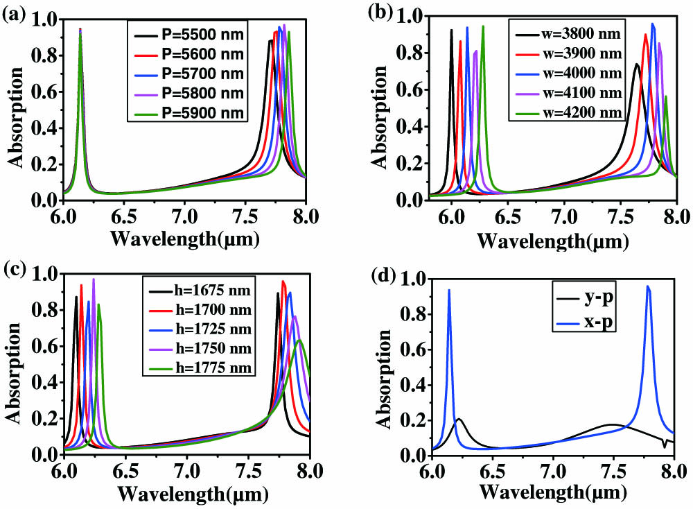
Fig. 2. Optical properties of the metastructure absorber. The graphs show the spectra of absorption with different (a) period
The absorbed electromagnetic radiation is converted into heat through Joule heating (resistive heat) following the Poynting’s theorem [43]. When our plasmonic absorber is under pulsed optical excitation, the temperature on the surface of the sensitive material will first rise and then fall. The heat transfer equation for our system reads
In the thermal simulation, we use AlN as the heat-sensitive material. All the relevant materials’ thermal parameters used in the simulation are shown in Table 1. AlN, a kind of pyroelectric material, possesses a temperature-dependent spontaneous polarization and on heating its polarization is altered [44]. AlN is well suited to ambient temperature operation when heated below its Curie temperature [45]. A current will be produced when the system is connected to an external circuit, due to the generation of pyroelectric voltage, which is caused by time-varying optical/thermal signals altering the density of the interfacial charges [44]. The red curve in Fig. 1(b) shows the normalized average increased temperature on the upper surface of AlN with wavelength changing. It can be seen that the surface temperature difference of the pyroelectric material AlN has a positive correlation with the absorption of the system; that is, the greater the absorption rate, the greater the and vice versa.
Table 1. Thermal Parameters of the Materials Used in Our Metastructures
|
In order to explore the application of this system in mid-infrared detectors, we take the first absorption peak, (the second absorption peak has a similar result), as an example (, , ) and investigate the temporal temperature distributions under different input conditions at this wavelength. First, we research the situation of different substrate materials, silicon (Si), silica (), and air, and the corresponding temporal temperature distributions are shown in Fig. 3(a) with the same incident flux . It can be clearly seen that when the substrate material is air (the system is suspended), the time required to rise to the same temperature is the shortest. In other words, the response of the suspended detector is the fastest, about 0.25 μs/K due to the smaller thermal conductivity, mass density, and specific heat capacity of air. Making the system suspended in the air is an effective way to improve the sensitivity of the detector [46]. In addition to the rise time, the total response time of the detector also includes the fall time, which is the time required for the detector to return to the initial state when the “heat source” is removed. Thus, the temporal temperature distributions of the suspended system under continuous wave (CW) and pulsed wave (PW) illumination are considered at the same incident flux (see Appendix E for the situations of the other two materials). The pulse function has the following form:
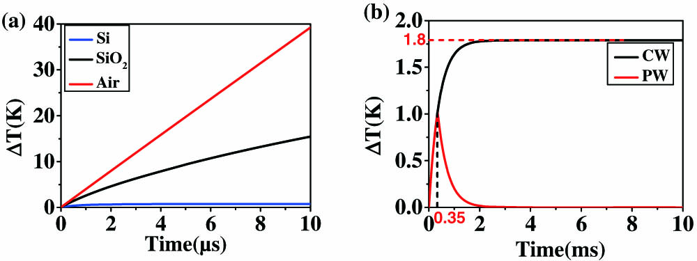
Fig. 3. Temporal temperature distributions for (a) different substrate materials with the same incident flux
Consecutively, the temporal temperature distributions for different pulse times and heat transfer coefficients at are investigated when the system is suspended, as shown in Figs. 4(a) and 4(b), respectively. Here, represents the heat exchange capacity between the interface and the surrounding environment, and the higher the value is, the stronger the heat dissipation capacity is (see Appendix A for more details). One can see that as the pulse time increases, keeps increasing, and the time for the detector to return to its initial state increases accordingly, until the system reaches a steady state. At this time, the total response time of the detector depends on the recognition of the minimum value of by the peripheral readout circuit. Different heat transfer coefficients will affect the total response time of the detector. From Fig. 4(b), a small will make the detector heat up quickly, and the cooling time (fall time) will be greatly increased. For example, when , the rise time is about 0.24 ms for , while the fall time is about 6.26 ms. Therefore, the designed detector must have good heat dissipation capacity to reduce the total response time.
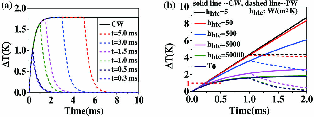
Fig. 4. Temporal temperature distributions for different (a) pulse time
Finally, we extend the proposed structure to unit cells, and the open boundary conditions are applied to replace the period boundary conditions. The temporal temperature distributions under CW and PW illumination are shown in Fig. 5. The total rise time (0.4 ms) and fall time (1.2 ms) are slightly larger than those in Fig. 3(b). The inset of Fig. 5 shows the maps of temperature distributions at . The proposed structure is very compact and can be easily fabricated by electron beam lithography [47], which provides the potential possibility for the practical application in the near future.
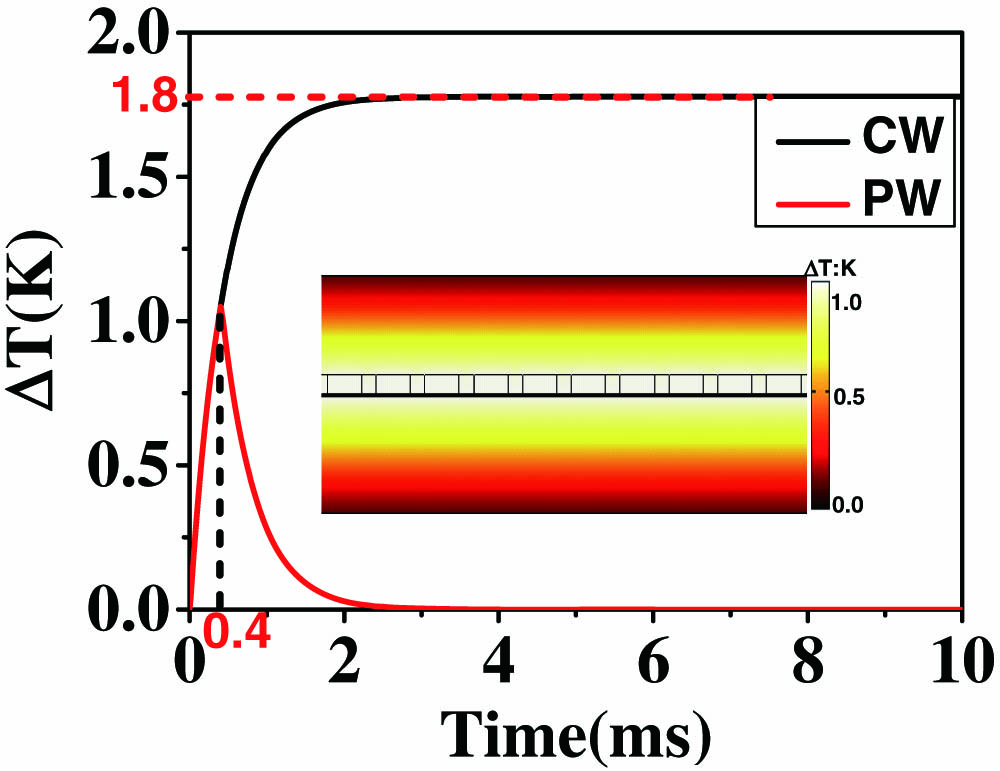
Fig. 5. Temporal temperature distributions for
3. CONCLUSION
In conclusion, we have demonstrated a dual-band PA for a mid-infrared photodetector based on a dielectric silicon metasurface, gold reflector, and pyroelectric material AlN. Simulation results show that the two narrowband perfect absorption peaks are achieved, and they can be easily tuned by controlling the structural parameters. In addition, the proposed system has good polarization selectivity, and the presence or absence of the second absorption peak can be controlled by altering the height of the Si-grating. The proposed system has higher heat conversion and heat transfer efficiency than traditional MIM structures. These physical features contribute to a fast total response time of about for dual-band and for single-band mid-infrared photodetectors at incident light flux . Our study provides direction and reference for the future design of high-sensitivity mid-infrared detectors.
[1] T. W. Ebbesen, H. J. Lezec, H. F. Ghaemi, T. Thio, P. A. Wolff. Extraordinary optical transmission through sub-wavelength hole arrays. Nature, 1998, 391: 667-669.
[2] F. J. García-Vidal, E. Moreno, J. A. Porto, L. Martín-Moreno. Transmission of light through a single rectangular hole. Phys. Rev. Lett., 2005, 95: 103901.
[3] Z. Ruan, M. Qiu. Enhanced transmission through periodic arrays of subwavelength holes: the role of localized waveguide resonances. Phys. Rev. Lett., 2006, 96: 233901.
[4] Y. Ling, L. Huang, W. Hong, T. Liu, J. Luan, W. Liu, J. Lai, H. Li. Polarization-controlled dynamically switchable plasmon induced transparency in plasmonic metamaterial. Nanoscale, 2018, 10: 19517-19523.
[5] Z. Chen, F. Zhang, Q. Zhang, J. Ren, H. Hao, X. Duan, P. Znag, T. Zhang, Y. Gu, Q. Gong. Blue-detuned optical atom trapping in a compact plasmonic structure. Photon. Res., 2017, 5: 436-440.
[6] S. Zhang, D. A. Genov, Y. Wang, M. Liu, X. Zhang. Plasmon-induced transparency in metamaterials. Phys. Rev. Lett., 2008, 101: 047401.
[7] N. I. Landy, S. Sajuyigbe, J. J. Mock, D. R. Smith, W. J. Padilla. Perfect metamaterial absorber. Phys. Rev. Lett., 2008, 100: 207402.
[8] X. Liu, T. Tyler, T. Starr, A. F. Starr, N. M. Jokerst, W. J. Padilla. Taming the blackbody with infrared metamaterials as selective thermal emitters. Phys. Rev. Lett., 2011, 107: 045901.
[9]
[10] Y. He, K. Lawrence, W. Lngram, Y. Zhao. Circular dichroism based refractive index sensing using chiral metamaterials. Chem. Commun., 2016, 52: 2047-2050.
[11] W. Wang, F. Yan, S. Tan, H. Zhou, Y. Hou. Ultrasensitive terahertz metamaterial sensor based on vertical split ring resonators. Photon. Res., 2017, 5: 571-577.
[12] Y. Zhao, A. Alu. Manipulating light polarization with ultrathin plasmonic metasurfaces. Phys. Rev. B, 2011, 84: 205428.
[13] Y. Zhao, M. Belkin, A. Alu. Twisted optical metamaterials for planarized ultrathin broadband circular polarizers. Nat. Commun., 2012, 3: 870.
[14] R. Ji, S. Wang, X. Liu, X. Chen, W. Li. Broadband circular polarizers constructed using helix-like chiral metamaterials. Nanoscale, 2016, 8: 14725-14729.
[15] A. K. Mikhail, C. Federico. Optical absorbers based on strong interference in ultra-thin films. Laser Photon. Rev., 2016, 10: 735-749.
[16] Z. Li, S. Butun, K. Aydin. Large-area, lithography-free super absorbers and color filters at visible frequencies using ultrathin metallic films. ACS Photon., 2015, 2: 183-188.
[17] J. Zhao, X. Yu, X. Yang, C. Augustine, W. Yuan, Y. Yu. Polarization-independent and high-efficiency broadband optical absorber in visible light based on nanostructured germanium arrays. Opt. Lett., 2019, 44: 963-966.
[18] Z. Li, W. Liu, H. Cheng, D. Choi, S. Chen, J. Tian. Spin-selective full-dimensional manipulation of optical waves with chiral mirror. Adv. Mater., 2020, 32: 1907983.
[19] I. Ozbay, A. Ghobadi, B. Butun, G. Turhan-Sayan. Bismuth plasmonics for extraordinary light absorption in deep sub-wavelength geometries. Opt. Lett., 2020, 45: 686-689.
[20] X. Liu, T. Starr, A. F. Starr, W. J. Padilla. Infrared spatial and frequency selective metamaterial with near-unity absorbance. Phys. Rev. Lett., 2010, 104: 207403.
[21] C. Wu, B. Neuner, J. John, A. Milder, B. Zollars, S. Savoy, G. Shvets. Metamaterial-based integrated plasmonic absorber/emitter for solar thermo-photovoltaic systems. J. Opt., 2012, 14: 024005.
[22] K. Aydin, V. E. Ferry, R. M. Briggs, H. A. Atwater. Broadband polarization-independent resonant light absorption using ultrathin plasmonic super absorbers. Nat. Commun., 2011, 2: 517.
[23] J. B. Chou, Y. X. Yeng, Y. E. Lee, A. Lenert, V. Rinnerbauer, I. Celanovic, M. Soljačić, N. X. Fang, E. N. Wang, S.-G. Kim. Enabling ideal selective solar absorption with 2D metallic dielectric photonic crystals. Adv. Mater., 2014, 26: 8041-8045.
[24] Y. Zhang, D. Meng, X. Li, H. Yu, J. Lai, Z. Fan, C. Chen. Significantly enhanced infrared absorption of graphene photodetector under surface-plasmonic coupling and polariton interference. Opt. Express, 2018, 26: 30862-30872.
[25] A. Safaei, S. Chandra, M. W. Shabbir, M. N. Leuenberger, D. Chanda. Dirac plasmon-assisted asymmetric hot carrier generation for room-temperature infrared detection. Nat. Commun., 2019, 10: 3498.
[26] T. D. Dao, S. Ishii, A. T. Doan, Y. Wada, A. Ohi, T. Nabatame, T. Nagao. An on-chip quad-wavelength pyroelectric sensor for spectroscopic infrared sensing. Adv. Sci., 2019, 6: 1900579.
[27] Z. Taghipour, S. Lee, S. A. Myers, E. H. Steenbergen, C. P. Morath, V. M. Cowan, S. Mathews, G. Balakrishnan, S. Krishna. Temperature-dependent minority-carrier mobility in p-type InAs/GaSb type-II-superlattice photodetectors. Phys. Rev. Appl., 2019, 11: 024047.
[28] T. D. Nguyen, J. O. Kim, Y. H. Kim, E. T. Kim, Q. L. Nguyen, S. J. Lee. Dual-color short-wavelength infrared photodetector based on InGaAsSb/GaSb heterostructure. AIP Adv., 2018, 8: 025015.
[29] S. Liu, M. Li, J. Zhang, D. Su, Z. Huang, S. Kunwar, J. Lee. Self-assembled Al nanostructure/ZnO quantum dot heterostructures for high responsivity and fast UV photodetector. Nano-Micro Lett., 2020, 12: 114.
[30] Y. F. Xiong, J. H. Chen, Y. Q. Lu, F. Xu. Broadband optical-fiber-compatible photodetector based on a graphene-MoS2-WS2 heterostructure with a synergetic photogenerating mechanism. Adv. Electron. Mater., 2019, 5: 1800562.
[31] J. Yao, G. Yang. 2D material broadband photodetectors. Nanoscale, 2020, 12: 454-476.
[32] L. Ye, P. Wang, W. Luo, F. Gong, L. Liao, T. Liu, L. Tong, J. Zang, J. Xu, W. Hu. Highly polarization sensitive infrared photodetector based on black phosphorus-on-WSe2 photogate vertical heterostructure. Nano Energy, 2017, 37: 53-60.
[33] M. W. Knight, H. Sobhani, P. Nordlander, N. J. Halas. Photodetection with active optical antennas. Science, 2011, 332: 702-704.
[34] W. Li, J. Valentine. Metamaterial perfect absorber based hot electron photo detection. Nano Lett., 2014, 14: 3510-3514.
[35] Y. Ho, Y. Tai, J. K. Clark, Z. Wang, P. Wei, J. Delaunay. Plasmonic hot-carriers in channel-coupled nanogap structure for metal-semiconductor barrier modulation and spectral-selective plasmonic monitoring. ACS Photon., 2018, 5: 2617-2623.
[36] T. D. Dao, K. Chen, S. Ishii, A. Ohi, T. Nabatame, M. Kitajima, T. Nagao. Infrared perfect absorbers fabricated by colloidal mask etching of Al–Al2O3–Al trilayers. ACS Photon., 2015, 2: 964-970.
[37] S. Kang, Z. Qian, V. Rajaram, S. D. Calisgan, A. Alu, M. Rinaldi. Ultra-narrowband metamaterial absorbers for high spectral resolution infrared spectroscopy. Adv. Opt. Mater., 2019, 7: 1801236.
[38] J. Park, J. Kang, S. J. Kim, X. Liu, M. L. Brongersma. Dynamic reflection phase and polarization control in metasurfaces. Nano Lett., 2017, 17: 407-413.
[39] S. Chen, Z. Chen, J. Liu, J. Cheng, Y. Zhou, L. Xiao, K. Chen. Ultra-narrow band mid-infrared perfect absorber based on hybrid dielectric metasurface. Nanomaterials, 2019, 9: 1350.
[40] G. Lan, Z. Jin, J. Nong, P. Luo, C. Guo, Z. Sang, L. Dong, W. Wei. Narrowband perfect absorber based on dielectric-metal metasurface for surface-enhanced infrared sensing. Appl. Sci., 2020, 10: 2295.
[41] J. Hao, L. Zhou, M. Qiu. Nearly total absorption of light and heat generation by plasmonic metamaterials. Phys. Rev. B, 2011, 83: 165107.
[42] F. Callewaert, S. Chen, S. Butun, K. Aydin. Narrow band absorber based on a dielectric nanodisk array on silver film. J. Opt., 2016, 18: 075006.
[43]
[44] J. W. Stewart, J. H. Vella, W. Li, S. Fan, M. H. Mikkelsen. Ultrafast pyroelectric photodetection with on-chip spectral filters. Nat. Mater., 2020, 19: 158-162.
[45] W. S. Yan, R. Zhang, X. Q. Xiu, Z. L. Xie, P. Han, R. L. Jiang, S. L. Gu, Y. Shi, Y. D. Zheng. Temperature dependence of the pyroelectric coefficient and the spontaneous polarization of AlN. Appl. Phys. Lett., 2007, 90: 212102.
[46] K. W. Mauser, S. Kim, S. Mitrovic, D. Fleischman, R. Pala, K. C. Schwab, H. A. Atwater. Resonant thermoelectric nanophotonics. Nat. Nanotechnol., 2017, 12: 770-775.
[47] L. Liu, X. Zhang, Z. Zhao, M. Pu, P. Gao, Y. Luo, J. Jin, C. Wang, X. Luo. Batch fabrication of metasurface holograms enabled by plasmonic cavity lithography. Adv. Opt. Mater., 2017, 5: 1700429.
Zhao Chen, Yudong Weng, Junku Liu, Nan Guo, Yaolun Yu, Lin Xiao. Dual-band perfect absorber for a mid-infrared photodetector based on a dielectric metal metasurface[J]. Photonics Research, 2021, 9(1): 01000027.
