飞秒激光辐照连接金属氧化物纳米线及电性能调控  下载: 1108次
Objective As the most common structural unit in electronic devices, the interface contact state of metal-semiconductor heterostructures plays an important role in the performance of electronic devices. Some traditional nanojoining technologies, such as ultrasonic nanojoining, joule heating, and ion and electron beam irradiation, have been used to improve the interface contact state of metal-semiconductor heterostructures. However, these methods easily cause additional damage to nanomaterials and require a complex processing environment, which poses a great challenge to the control of energy inputs. Femtosecond lasers with short pulse time and high peak intensity, as a method of nanojoining, are suitable to process nanomaterials with high melting points and damage thresholds. In recent years, most research studies have focused on the fabrication of metal-semiconductor heterostructure devices using femtosecond laser technology, but the material systems need to be broadened. In this study, the dry transfer method is used to fabricate Au electrode-CuO/ZnO nanowires (NWs) heterostructures and a semiconductor inverter based on p-type CuO NWs and n-type ZnO NWs. The nanojoining of the heterostructures based on the localized energy input of femtosecond lasers caused by the surface plasmon effect is successfully realized. The laser-treated semiconductor inverter had obtained stable voltage regulation capability based on the p-type and n-type field-effect transistor characteristics of CuO and ZnO NWs. This study provides a new idea for the top-down assembly of micro/nanoelectronic devices. We hope that our design provides a new idea for the top-down assembly of micro/nanoelectronic devices.
Methods CuO nanowires (NWs) were synthesized by thermal oxidation at 400 ℃ for 4 h; however, ZnO NWs and lithography electrodes were purchased directly from XFNANO Materials. Au electrode-CuO/ZnO NWs heterostructures and a semiconductor inverter based on p-type CuO NWs and n-type ZnO NWs were fabricated using a continuous dry transfer method. The nanojoining of the heterostructures was achieved using femtosecond laser irradiation (50 fs pulse duration, 800 nm wavelength, and 1 kHz frequency). The surface morphology and crystalline structure of nanowires were analyzed using scanning electron microscopy (SEM, Zeiss Supra 55) and X-ray diffraction (XRD, Bruker D8). The electrical characterization of the heterostructures and the semiconductor inverter in a three-terminal configuration were examined by a probe station (Keithley 2636B). In addition, the commercial finite element analysis (COMSOL Multiphysics 5.4) was used to simulate the electric ?eld distribution of the heterostructures under linearly polarized Gauss light to further elucidate the interfacial modification mechanism of Au electrode-CuO/ZnO under femtosecond lasers.
Results and Discussions The stable welded joints of the Au electrode-CuO/ZnO NWs heterostructures are obtained by femtosecond laser irradiation with a power intensity of 12.9 mJ/cm 2 and 20.2 mJ/cm 2, respectively. The nanowires form a degree of wetting angle on the surface of the Au electrode (the red dotted line area), and the surface organic matter is effectively removed, greatly improving the interface contact state (Fig. 4). The simulation results show that the enhancement region with a high electric field intensity mainly occurred in the interface between the Au electrode and nanowires on both sides, while the suspended nanowires in the middle have lower electric field intensity (Fig. 5). The strong surface plasmon effect due to femtosecond laser irradiation confines the energy to the interface of the heterostructures, promoting the formation of low damage welded joints. Compared with the electrical measurement results of pristine and laser-treated heterostructures, the voltage dependence of the p-type and n-type NW field-effect transistors (FETs) irradiated by femtosecond lasers is significantly improved. When the gate voltage (VG) reaches +20 V and -20 V, there is an obvious trend of current suppression for CuO and ZnO NWs, respectively (Fig. 6). In addition, the semiconductor inverter is fabricated based on the p-type and n-type FET characteristics of the CuO and ZnO NWs (Fig. 7). The laser-treated inverter had obtained stable voltage regulation capability, with a full voltage output swing of ~79.5% (Fig. 8).
Conclusions In this study, the Au electrode-CuO/ZnO NWs heterostructures are successfully fabricated through the dry transfer method. The strong plasmon interaction of metal-semiconductor heterostructural interface induced by femtosecond laser irradiation is demonstrated using COMSOL multi-physical field simulation to elucidate nanojoining mechanism. The laser energy is effectively limited in the interface area between the Au electrode and nanowires, achieving a low damage nanojoining of the heterogeneous materials. The device units of the two kinds of nanowire heterostructures have obvious electrical characteristics of p-type and n-type FETs with a great back gate control performance. The laser-treated semiconductor inverter had obtained stable voltage regulation capability based on p-type CuO NWs and n-type ZnO NWs, with a full voltage output swing of ~79.5%. The fabrication of Au electrode-CuO/ZnO nanowires heterostructures through dry transfer and femtosecond laser irradiation extends the material systems of metal-semiconductor heterostructures. In the end, we hope that the design of the inverter provides a new idea for the top-down assembly of micro/nanoelectronic devices.
1 引言
随着微电子领域的迅猛发展,以半导体为基础的芯片产业对电子器件的性能提出了更高的要求,器件逐渐偏向小尺度、高集成度以及多功能材料体系发展,材料逐渐进入纳米尺度范围,通过改善结构实现具有复杂纳米结构(跨尺度、维度)的电子器件也成为当前研究的热点[1]。
金属-半导体异质结构是电子器件中最常见的结构单元,其界面结合状态对于器件的性能尤为重要[2]。但实际情况中,金属与半导体相互接触时,有机物等杂质会严重影响器件的性能[3]。超声焊[4]、退火法[5]、离子束[6]和电子束[7]等均可被用以改善金属-半导体异质界面的接触状态,但这些方法往往会对纳米材料造成过损伤,加工环境也比较复杂。因此,在异质材料界面结构连接时,不仅要避免纳米材料的过损伤,还需在一定程度上去除杂质、有机物,对能量输入的控制提出了极大的挑战。
飞秒激光作为纳米连接的一种方法,具有脉冲时间短、峰值强度高、与材料相互作用时热量输入少等特点,可适用于高熔点和高损伤阈值纳米材料的加工[8-9]。此外,对于光辐照下的金属-半导体异质界面,表面等离子激元效应的存在使能量输入在异质界面呈周期性热点分布[10]。Lin等[11-12]采用飞秒激光实现了多种金属-半导体异质结构材料体系的界面调控,包括Au电极-TiO2纳米线(NWs)、Ag纳米线-TiO2纳米线,可应用于多级忆阻器等器件。Cui等[13]使用飞秒激光实现了碳纳米管与Ni电极的欧姆接触。Xing等[14]使用飞秒激光实现了Pt电极-TiO2纳米线异质结构的互连,可模拟长时记忆特性的神经网络单元。近年来,采用飞秒激光作为制备和调控金属-半导体异质界面结构器件的方法受到了广泛关注,但材料体系仍有待拓宽。CuO和ZnO纳米线分别作为一种典型的p型和n型半导体,具有优异的电学特性,因此,被广泛应用于多种电子器件,但较大的界面接触电阻严重阻碍了其电学应用。因此,获得稳定的金属电极-CuO/ZnO纳米线互连结构具有重要意义。
本文基于金属-半导体异质结构体系的研究,用干法转移方法构造了Au电极-CuO/ZnO纳米线异质结构,探究了基于飞秒激光辐照的异质结构界面互连行为,并利用多物理场有限元模拟软件(COMSOL Multiphysics 5.4)揭示异质界面的表面等离子激元强化效应,从而解释激光的连接机理。通过对比异质结构辐照前后的电学特性,研究异质结构界面的状态变化对场效应管(FET)器件性能的影响。此外,基于p-CuO和n-ZnO纳米线的FET电流调控特性,制备了一种半导体倒相器,并研究了激光辐照前后该器件的电压调控能力。
2 实验材料及方法
2.1 实验材料
CuO纳米线采用热氧化法合成,首先,将工业纯Cu网用盐酸去除表面的氧化膜后置于管式炉中,在450 ℃氧气环境下保温4 h。然后,将氧化后的Cu网置于装有酒精溶液(纯度大于等于99.7%)的烧杯中,超声振荡10 s后得到CuO纳米线酒精悬浮液。将购买的ZnO纳米线用相同的酒精稀释,得到悬浮液。器件使用的Au电极及基板采用微电子光刻等工艺制备。
2.2 器件制备
采用干法转移方法制备Au电极-纳米线异质结构和倒相器[15-16],其流程如
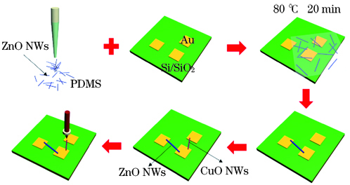
图 1. 干法转移方法制备的Au电极-纳米线异质结构
Fig. 1. Au electrode-nanowire heterostructure prepared by dry transfer method
2.3 飞秒激光加工系统
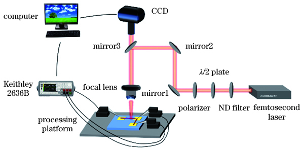
实验用功率为4 W的钛宝石飞秒激光器(美国相干公司)作为光源辐照纳米线与电极,激光器的波长为800 nm,脉冲宽度为50 fs,重复频率为1 kHz。如
2.4 器件性能表征
纳米线的形貌用扫描电镜(SEM, Zeiss Supra 55)和光学显微镜(OM)表征。此外,用X射线衍射仪(XRD, Bruker D8)对纳米线进行物相分析,用能谱仪(EDS)探测其表面的化学元素分布,用四探针精密半导体电学测试仪器(Keithley 2636B)测量CuO和ZnO纳米线的FET及倒相器的电学特性。实验用COMSOL Multiphysics 5.4软件表征CuO和ZnO纳米线与Au电极之间的电势场分布,探究飞秒激光对金属-半导体异质界面的修饰机理。多物理场模拟基于射频模块进行建模,入射光的波长为800 nm,初始入射电场强度为1 V/m。
3 分析与讨论
3.1 Au电极-CuO/ZnO纳米线异质结构的界面互连
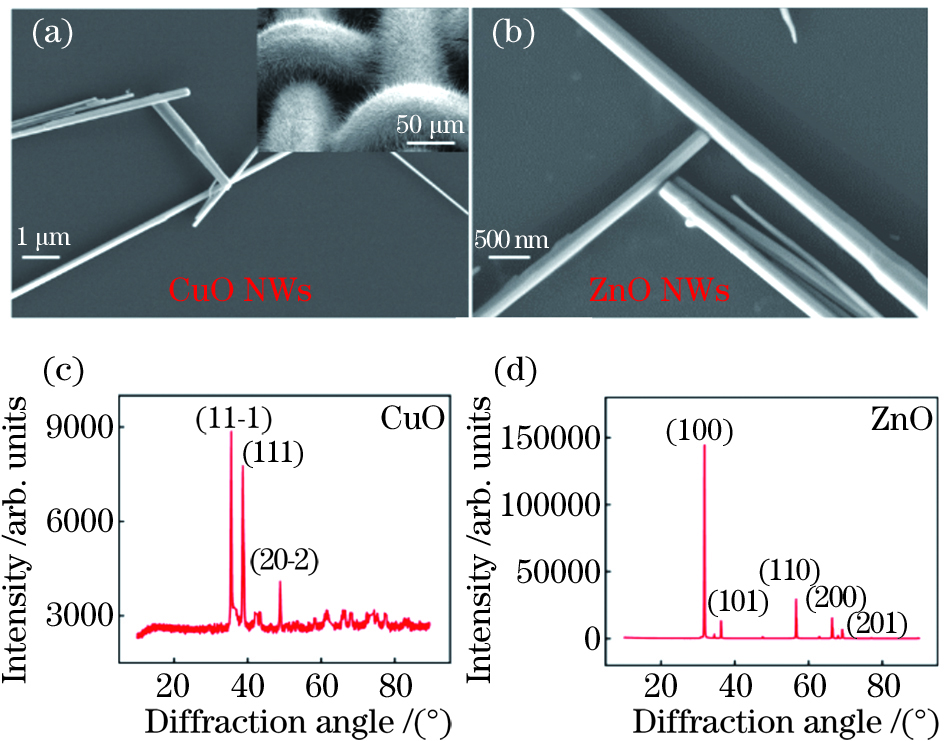
图 3. 纳米线的表面形貌和物相结构。(a)CuO纳米线的SEM图像;(b)ZnO纳米线的SEM图像;(c)CuO纳米线的X射线衍射图谱;(d)ZnO纳米线的X射线衍射图谱
Fig. 3. Surface morphology and phase structure of the nanowires. (a) SEM image of the CuO nanowires; (b) SEM image of the ZnO nanowires; (c) X-ray diffraction pattern of the CuO nanowires; (d) X-ray diffraction pattern of the ZnO nanowires
Au电极与纳米线异质结构互连属于跨尺度的纳米连接,材料的本征属性和异质结构的几何接触形态会严重影响飞秒激光辐照下界面行为的转变,从而影响异质结构的互连状态[17]。
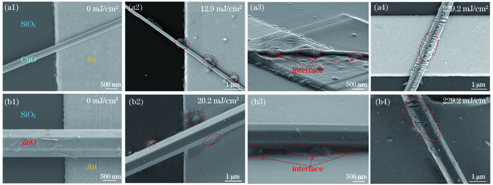
图 4. 异质结构在不同激光能量辐照下的接头形貌。(a) Au电极-CuO纳米线异质结构;(b) Au电极-ZnO纳米线异质结构
Fig. 4. Joint morphology of the heterostructure under different laser energy irradiation. (a) Au electrode-CuO nanowire heterostructure; (b) Au electrode-ZnO nanowire heterostructure
激光辐照金属与介电材料界面时,金属表面的自由电子会发生振荡,形成能量分布的热点区域,即表面等离子激元效应[18-19]。为了研究飞秒激光辐照下Au电极-纳米线异质结构的界面电场分布,采用COMSOL Multiphysics 5.4软件依据实际尺度构造了简化的Au电极-纳米线异质结构模型,主要包括两侧的Au电极-纳米线搭接区域和中部的悬空纳米线-空气接触区域,模拟条件为均匀空间电磁场。如
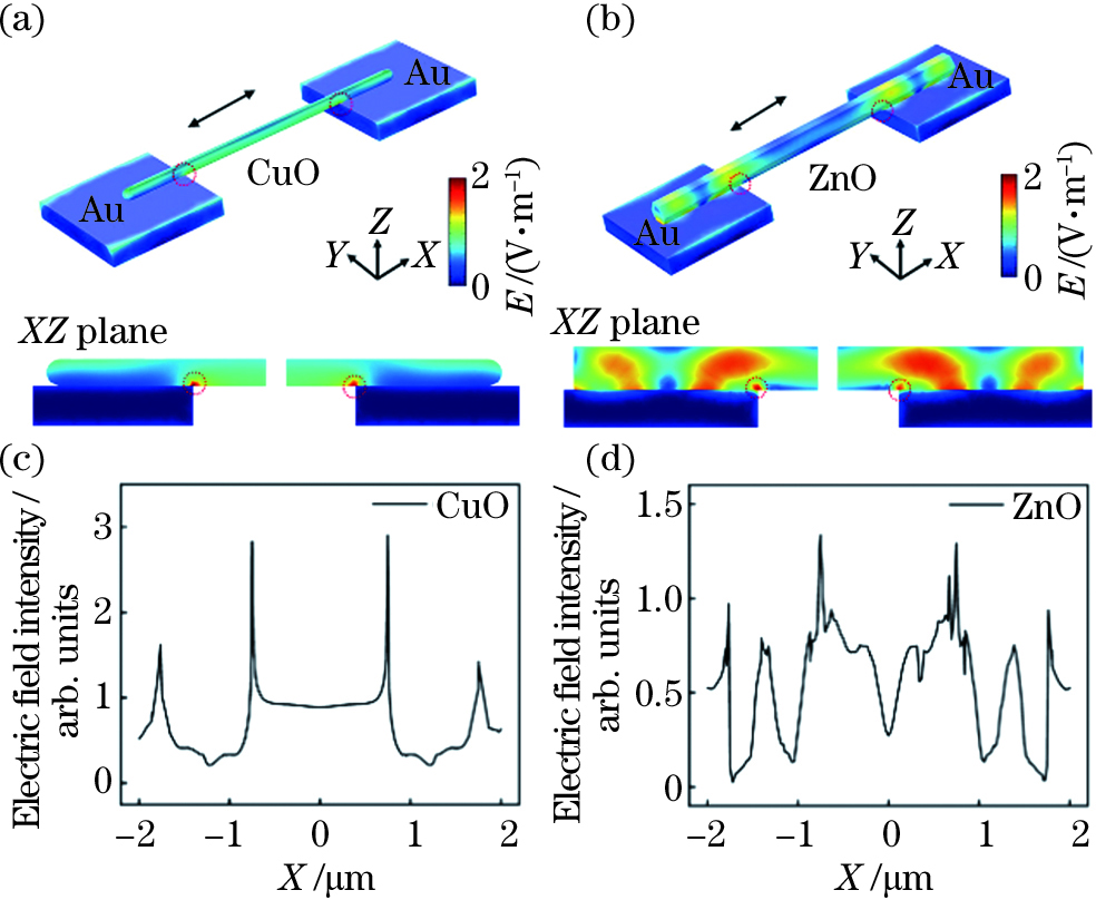
图 5. 激光辐照下的电场强度分布。(a)Au电极-CuO纳米线;(b)Au电极-ZnO纳米线;(c)沿CuO纳米线轴与电极接触面的电场强度;(d)沿ZnO纳米线轴与电极接触面的电场强度
Fig. 5. Electric field intensity distribution under laser irradiation. (a) Au electrode-CuO nanowires; (b) Au electrode-ZnO nanowires; (c) electric field strength along the CuO nanowire axis and electrode contact surface; (d) electric field strength along the ZnO nanowire axis and electrode contact surface
3.2 Au电极-CuO/ZnO纳米线异质连接结构的电学特性
干法转移方法制备的Au电极-纳米线异质结构受飞秒激光辐照后,其界面接触状态会发生明显改变,进而影响其电学特性。
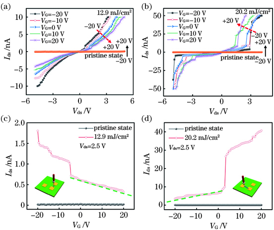
图 6. 纳米线与Au电极连接前后的电学响应。(a)、(c)激光辐照前后CuO纳米线FET器件的电流输出特性和转移特性;(b)、(d)激光辐照前后ZnO纳米线FET器件的电流输出特性和转移特性
Fig. 6. Electrical response before and after the nanowire is bonded to the Au electrode. (a),(c) Current output characteristics and transfer characteristics of the CuO nanowire FET devices before and after laser irradiation; (b),(d) current output characteristics and transfer characteristics of the ZnO nanowire FET devices before and after laser irradiation characteristic
3.3 p-CuO/n-ZnO纳米线倒相器的飞秒激光纳米连接
CuO和ZnO纳米线作为一种典型的半导体材料,具有优异的电学性能,被广泛应用于多种电子器件中[20]。基于p-CuO和n-ZnO纳米线FET的电学特性可知,其漏源电流随栅极电压的变化趋势不同,实验采用干法转移方法制备了p-CuO/n-ZnO纳米线半导体倒相器,器件模型如
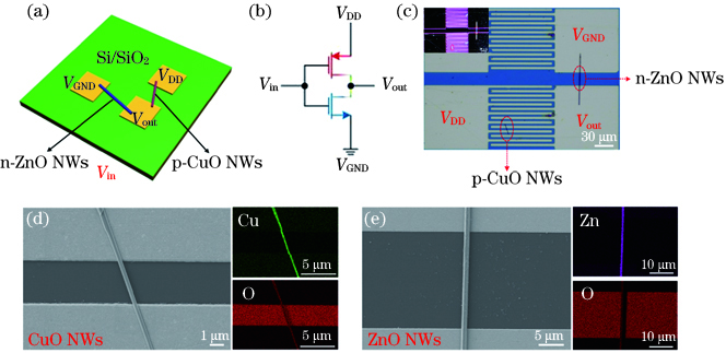
图 7. 基于p-CuO/n-ZnO纳米线的半导体倒相器。(a)倒相器结构示意图;(b)电路原理图;(c) OM图像;(d) p-CuO纳米线FET的SEM图像及EDS表征;(e) n-ZnO纳米线FET的SEM图像及EDS表征
Fig. 7. Semiconductor inverter based on p-CuO/n-ZnO nanowires. (a) Schematic structure of the inverter; (b) schematic circuit diagram; (c) OM image; (d) SEM image and EDS characterization of the p-CuO nanowire FET devices; (e) SEM image and EDS characterization of the n-ZnO nanowire FET devices
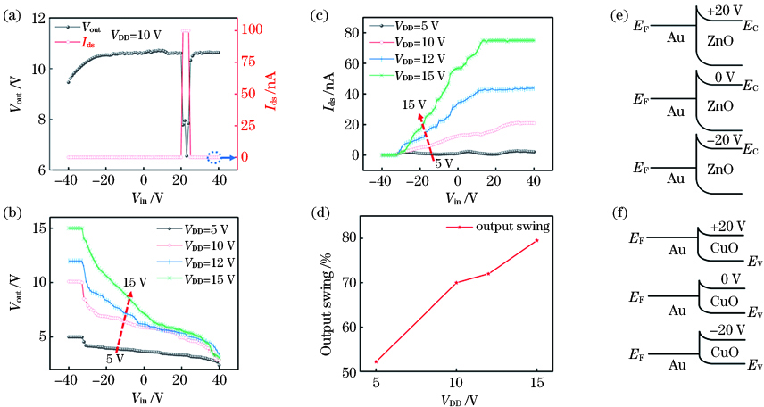
图 8. 倒相器的电学响应特征及能带结构。(a)初始状态倒相器的电压和电流传输曲线;(b)~(c)激光处理后倒相器的电压和电流传输曲线;(d)不同电源电压下倒相器的电压调控幅度变化;(e)~(f)p-CuO和n-ZnO纳米线FET在不同栅极电压下的能带结构
Fig. 8. Electrical response characteristics and energy band structure of the inverter. (a) Voltage and current transfer curve of the inverter in the initial state; (b)--(c) voltage and current transfer curves of the inverter after laser processing; (d) voltage regulation range of the inverter under different applied voltages; (e)--(f) energy band structure of p-CuO and n-ZnO nanowire FET under different gate voltages
4 结论
采用干法转移方法成功制备出了Au电极-CuO/ZnO纳米线异质结构,并利用COMSOL Multiphysics 5.4软件揭示了飞秒激光辐照下金属-半导体异质界面产生的表面等离子激元效应。实验结果表明,能量被有效限制在Au电极与纳米线接触区域,从而实现Au电极与CuO/ZnO纳米线的低损伤连接。两种纳米线互连结构的器件单元分别具有明显的p型和n型FET电学特性,背栅调控性能明显。基于此制备了一种p-CuO/n-ZnO纳米线半导体倒相器,实验结果表明,激光处理后的器件获得了稳定的电压调控能力,其电压的调控范围最大为79.5%。干法转移方法和飞秒激光制备Au电极-纳米线互连结构拓宽了金属-半导体异质界面多材料体系,制备的倒相器为自下而上的微纳电子器件组装提供了一种新思路。
[6] Krasheninnikov A V, Nordlund K, Keinonen J. Production of defects in supported carbon nanotubes under ion irradiation[J]. Physical Review B, 2002, 65(16): 165423.
[9] 廖嘉宁, 王欣达, 周兴汶, 等. 飞秒激光直写铜微电极研究[J]. 中国激光, 2019, 46(10): 1002013.
[13] Cui J L, Cheng Y, Zhang J W, et al. Femtosecond laser irradiation of carbon nanotubes to metal electrodes[J]. Applied Sciences, 2019, 9(3): 476.
[17] 郭敏超, 王明娣, 张胜江, 等. FR-4覆铜板飞秒激光微孔加工工艺研究[J]. 中国激光, 2020, 42(12): 1202008.
[19] 滕达, 赵永哲, 王云成, 等. 基于硅-绝缘体结构的石墨烯等离激元波导[J]. 激光与光电子学进展, 2020, 58(3): 032301.
Teng D, Zhao Y Z, Wang Y C, et al. Graphene plasmonic waveguide based on silicon-on-insulator structures[J]. Laser & Optoelectronics Progress, 2020, 58(3): 032301.
[20] Meng J P, Li Z. Schottky-contacted nanowire sensors[J]. Advanced Materials, 2020, 32(28): 2000130.
Article Outline
孙天鸣, 肖宇, 霍金鹏, 沈道智, 王文先, 邹贵生. 飞秒激光辐照连接金属氧化物纳米线及电性能调控[J]. 中国激光, 2021, 48(8): 0802006. Tianming Sun, Yu Xiao, Jinpeng Huo, Daozhi Shen, Wenxian Wang, Guisheng Zou. Nanojoining and Electrical Performance Modulation of Metal Oxide Nanowires Based on Femtosecond Laser Irradiation[J]. Chinese Journal of Lasers, 2021, 48(8): 0802006.
