银纳米材料的纳连接及其电学性能研究  下载: 998次
Objective Owing to the increasing demand for microelectronic devices, micro-nanostructures obtained using nanomaterials have great advantages in reducing size and achieving characteristic performance. Because a structure characteristic size is reduced to the nanoscale, its light absorption, melting point, and several other physical and chemical properties are different from macroscopic bulk materials, demonstrating the unique size effect of nanomaterials. Therefore, nanojoining often requires low-energy conditions. Chemical, light, electrical, and thermal energies can be used as energy sources to achieve the low-temperature or room-temperature joining of nanomaterials. To date, the methods to achieve nanojoining mainly include self-joining, thermal sintering, and laser sintering. In this study, the performance of the abovementioned three methods in joining silver nanomaterials was evaluated. The electrical properties and microstructure of silver nanomaterials under different joining methods were compared, and the potential joining mechanism was analyzed. Laser sintering, with the advantages of high precision, high efficiency, and low damage to a substrate, is applied in flexible device preparation, dissimilar material combination device preparation, and electronic packaging.
Methods Silver nanomaterials (Ag NP) were obtained by the hydrothermal method. A mixture of 30-mL AgNO3 aqueous solution (5.1-g AgNO3) with 200-mL glucose (14 g) and PVP (8 g) aqueous solution was heated to 90 ℃ for 20 min under vigorous stirring and then naturally cooled. After the ultrasonication and centrifugation of the reaction solution, the solid matter was extracted and dried at 50 ℃ to obtain silver nanomaterials.
Silvernanobelts were synthesized by a one-step solution method at ambient temperature (~25 ℃). The aqueous solution of AgNO3 (4 mol/L,5 mL) was successively added to the aqueous solution of VC (0.25 mol/L,20 mL) and PMAA-Na (mass fraction of 30%,5 μL). The mixture was then washed using water, and the solid material was extracted after centrifugation to obtain the silver nanobelts.
Moreover, the conductive inks (solid content with mass fraction of 30%) with different quantities of silver nanobelts were prepared. Two materials, glass and PI films, were used as substrates. Electrodes were printed using a direct writing platform. Laser sintering was performed using an 808-nm diode laser with a spot diameter of 600 μm and a constant power density of 15.3 W/mm2. Their morphologies were characterized using a scanning electron microscope (SEM, Merlin Compact, Germany) and a transmission electron microscope (TEM, JEOL 2100F, Japan). Resistance of the silver structure was measured using a source meter (Keithley, 2400), and the electrode resistivity σ was calculated using σ=RS/L, where R is measured resistance, S is cross-sectional area, and L is the length of the electrodes. The 20-mm electrodes were used for bending tests using a homemade bending device. The bending frequency was 30 cycles/min, bending degree was 50%, and bending speed was 10 mm/s.
Results and Discussions Chemical energy of a reduction reaction can drive silver nanomaterials to self-join. The self-joined structure was composed of a large number of silver nanobelts with a smooth surface (
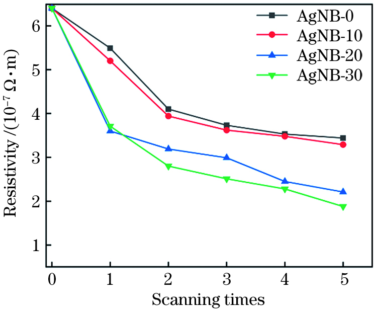
Conclusions In this study, the performance of the three methods, including self-joining, thermal sintering, and laser sintering, in the joining of silver nanomaterials was evaluated. The electrical properties and microstructure of the silver nanomaterials under different joining methods were compared. Although self-joining can promote the joining of nanoparticles at room temperature(~25 ℃), it results in a large number of dielectric substances in a system. The resistivity of the self-joined structure was 5.56×10⁻⁵ Ω·m and that of the nanobelt electrodes after thermal sintering was 5.4×10⁻⁷ Ω·m. However, the sintered structure was uncontrollable at high temperatures and not suitable for flexible substrates. In contrast, laser sintering can induce the joining of silver nanomaterials at low temperatures without destroying a substrate. Under the laser irradiation, the silver nanobelts were interconnected to form a network structure, electrode resistivity was 1.88×10⁻⁷ Ω·m, and electrode resistance change rate was 21.26% after 3000 bending cycles.
1 引言
随着电子器件向着微型化、集成化、轻量化、便携化方向发展,器件内部结构尺寸逐渐缩小至微米至纳米量级,传统“宏”机械制造技术已不能满足这些“微”机械和“微”系统高精度制造和装配加工的要求,必须开发微纳制造的技术与方法[1-2]。微纳制造技术是微传感器、微执行器、微结构和功能微纳系统制造的基本手段和重要基础[3]。其中,微纳米尺度的连接技术已成为从纳米材料构筑微纳结构的有效途径。由于待连接结构尺寸缩小到纳米尺度后,其光吸收性、熔点等许多物理化学性质与宏观块材有很大区别,表现出纳米材料独有的尺寸效应、微结构的表面效应等[4],这使得纳米尺度的连接往往对能量条件要求较低,化学能、光能、电能、热能等途径均能作为能量来源[5-8],实现纳米材料的低温甚至室温连接[9-10]。
传统热烧结是“自下而上”制备微电极等微纳结构的常用手段之一,通过烧结可将原本分散的材料连接为整体结构,获得良好的电学及机械性能。Li等[11]按摩尔比2∶1(Cu∶Ag)配置了纳米银铜导电膏,在250 ℃,1.12 MPa,Ar-H2气氛下实现了纳米材料的连接,所得的导电膏电阻率为1.99×10⁻⁷ Ω·m,最大剪切强度为25.4 MPa。Wang等[12]使用热烧结对直写电极内的银纳米颗粒进行连接,该电极经90 ℃,15 min热烧结后电阻率降到1.2×10⁻⁷ Ω·m。但受限于基底材料,热烧结不适用于柔性基底[13]。采用化学方法对纳米材料进行局域修饰,还可实现纳米材料的自组装及自连接。Peng等[14]使用去离子水清洗包裹在银纳米线表面的有机物保护膜,裸露的银纳米线表面具有高表面能,在表面能的驱使下,界面处的原子经扩散形成金属键合,实现了纳米线在室温下的自连接。Marzbanrad等[15]在液体环境中将银盐前驱体还原为银纳米片,并在结构导向剂聚甲基丙烯酸的作用下实现银纳米片的自组装连接,得到银纳米带。
热烧结虽适用于大面积连接但烧结条件通常较苛刻,而自连接无法进行精细操控,难以大范围应用。激光作为一种能量的承载形式,在激光辐照银纳米颗粒时,等离子激元效应诱导在纳米结构不连续处产生局部“热点”[16],使得该部位的能量远高于其他位置[17],利用该能量可促使纳米材料边界的原子扩散,能够在近室温下消除边界实现互连的同时保持纳米结构完整性[18]。由于激光烧结具有高精度、高效率、低损伤的优势,在柔性器件制备、异种材料组合器件制备、电子封装等领域有望得到应用[19-20]。本文采用银纳米颗粒、纳米带制备不同导电电极,研究了自连接、热烧结、激光烧结三种连接方式对银纳米材料的微观结构及其导电性能的影响,并对各连接方式的连接机理进行了探究。
2 实验部分
2.1 原料及试剂
实验所需试剂包括硝酸银、聚甲基丙烯酸钠(PMAA)、抗坏血酸(VC)、聚乙烯吡咯皖酮(PVP)、葡萄糖、氢氧化钠、聚乙二醇(PEG)等。所用化学药品均为分析纯,全部购自国药集团化学试剂有限公司。实验用水为去离子水。
采用水热法制备银纳米颗粒(AgNP),将200 mL水、14 g葡萄糖、8 g PVP混合均匀,所得溶液加热至90 ℃,逐滴加入30 mL 1 mol/L的硝酸银溶液,并伴随转子搅拌。90 ℃保温20 min后自然冷却。反应溶液经超声和离心后,提取固体物质,并使其在50 ℃下烘干,得到银纳米颗粒。
采用室温下的液相还原法制备银纳米带(AgNB),将5 mL硝酸银(4 mol/L)溶液加入到20 mL抗坏血酸(0.25 mol/L)与聚甲基丙烯酸钠(5 μL,质量分数为30%)的混合溶液中,得到银纳米带悬浊液。静置片刻,用去离子水洗涤沉淀,离心后提取固体物质,得到银纳米带。
2.2 实验步骤及仪器设备
固定固体物质的含量(质量分数w为30%), 制备具有不同银纳米带含量的导电油墨,油墨成分见
表 1. 导电油墨成分
Table 1. Contents of conductive inks
|
3 分析与讨论
湿化学法制备得到的纳米颗粒表面均匀包裹PVP薄膜[21],可确保纳米颗粒在保存过程中不团聚变质,其平均粒径约为72 nm,如

图 1. 合成纳米材料表面形貌。(a)银纳米颗粒;(b)银纳米带
Fig. 1. Morphology of synthesized silver. (a) Nanoparticles; (b) nanobelts
3.1 银纳米颗粒的自连接
当没有额外能量输入时,仅依靠化学反应自身的化学能可驱动银纳米材料的自发连接[22]。在纳米带的制备过程中,使用无水乙醇迅速稀释反应溶液,可中断反应过程,从而提取反应初期产物并观察其微观形貌,如
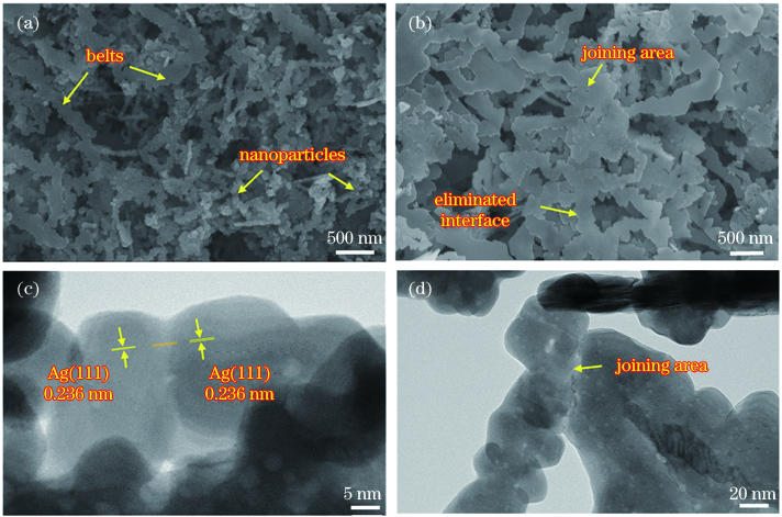
图 2. 银纳米颗粒的自连接。(a)连接初期连接界面的SEM照片;(b)连接后期连接界面的SEM形貌图;(c)纳米片沿(111)晶面定向连接界面的TEM照片;(d)纳米带间的连接界面的TEM照片
Fig. 2. Self joining of silver nanoparticles. (a) SEM image of the reaction product taken from early stage; (b) SEM image of the reaction product after joining; (c) TEM image of three silver nanoparticles after joining, in which directions of (111) planes of the particles are marked; (d) TEM image of joining interface of two silver nanobelts
3.2 银纳米带的热烧结
为研究银纳米带的烧结性能,将银纳米带制成导电油墨,经微笔直写在玻璃上制备出银纳米带电极。由
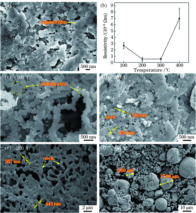
图 3. 银纳米带的热烧结。(a)烧结前微观形貌;(b)烧结温度对电极电阻率的影响;(c)~(f)不同烧结温度(100,200,300,400 ℃)下电极微观形貌
Fig. 3. Thermal sintering of silver nanobelts. (a) SEM image of the unsintered electrodes; (b) resistivity as a function of sintering temperature; (c)--(f) SEM images of electrodes sintered after 100, 200, 300, 400 ℃
3.3 银纳米带/颗粒的激光烧结
利用不同质量分数的银纳米带填料制备导电油墨,并用其在柔性聚酰亚胺基底上直写获得电极。接着探索激光对这些电极的烧结行为。各电极电阻率随激光扫描次数的变化如
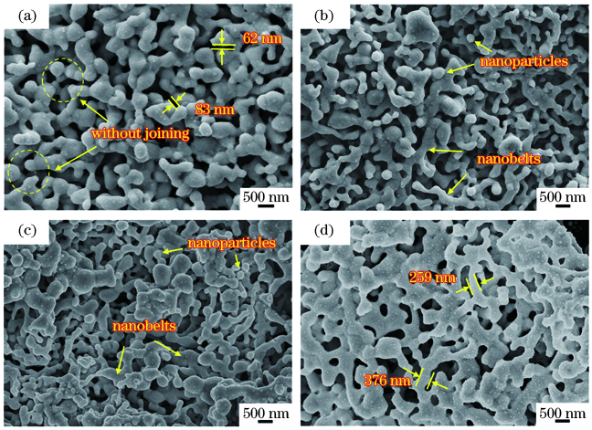
图 5. 激光烧结后各电极微观扫描电镜形貌。(a) AgNB-0; (b) AgNB-10; (c) AgNB-20; (d) AgNB-30
Fig. 5. SEM images of laser sintered electrodes. (a) AgNB-0; (b) AgNB-10; (c) AgNB-20; (d) AgNB-30
采用自制装置对激光扫描5次后各直写电极的抗弯折稳定性进行了测试,评价了各电极弯折后的电阻变化率K,其中K=(R-R0)/R0,R为弯折后电阻,R0为电极初始电阻。激光烧结后聚酰亚胺上直写的电极与基体的结合力较好,其中纳米带在抵抗剧烈弯折变形中有着更大的优势,电极抗弯折性能随银纳米带含量的增加而增强。在3000个弯折循环后,纯纳米颗粒电极电阻变化达164.88%,而与之相比,纳米带质量分数为10%、20%、30%的电极电阻变化分别为108.92%、59.05%、21.26%[
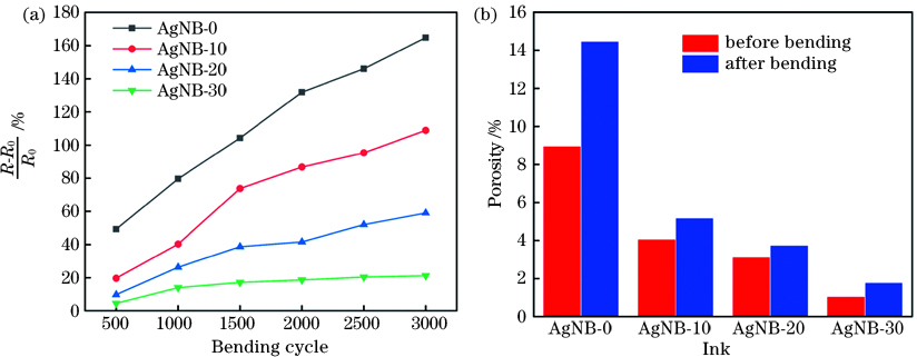
图 6. 电极弯折测试。(a)弯折次数对电极电阻变化率的影响;(b)经3000次弯折前后电极孔隙率对比
Fig. 6. Bending tests of sintered electrodes. (a) Influence of bending cycles on rate of electrode resistance; (b) comparison of electrode porosity before and after 3000 bending
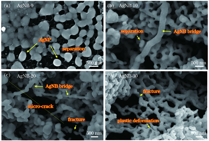
图 7. 经3000次弯折后各电极微观形貌。(a) AgNB-0; (b) AgNB-10; (c) AgNB-20; (d) AgNB-30
Fig. 7. SEM images of electrodes after 3000 bending cycles. (a) AgNB-0; (b) AgNB-10; (c) AgNB-20; (d) AgNB-30
综上所述,自连接、热烧结、激光烧结三种不同的连接方式,均可不同程度实现银纳米材料的连接。其中,自连接的工艺简便,且对能量要求较低,但其连接程度较弱,连接过程中不可控因素较多;热烧结适合大面积连接,但烧结通常需较高温度且对柔性基底的要求较高;激光烧结具有效果好、效率高、烧结结构可调控、适用于柔性基底等优势,尤其在纳米材料的选区高精度连接中有着较好的应用前景。
4 结论
研究了银纳米材料在制备过程中的自连接过程,对比研究了热烧结及激光连接后银电极的微观结构及其电学性能。自连接虽可促使室温下纳米颗粒的连接,但该方法却在体系内残留了大量介电物质,连接后电阻率为5.56×10⁻⁵ Ω·m,纳米带之间连接程度较弱。热烧结后的纳米带电极电阻率低至5.4×10⁻⁷ Ω·m,但高温下烧结结构不可控且对基底要求较高。相比而言,激光烧结可在避免基底损伤的同时诱导银纳米材料在低温下连接,进而得到电学、机械性能良好的电极。在激光诱导下,银纳米带间实现互连形成网络结构,电极电阻率低至1.88×10⁻⁷ Ω·m,且经3000次弯折后电极的电阻变化率仅为21.26%。
[1] Arafat M M, Dinan B, Akbar S A, et al. Gas sensors based on one dimensional nanostructured metal-oxides: a review[J]. Sensors (Basel), 2012, 12(6): 7207-7258.
[2] Duan X, Huang Y, Cui Y, et al. Indium phosphide nanowires as building blocks for nanoscale electronic and optoelectronic devices[J]. Nature, 2001, 409(6816): 66-69.
[3] Li L, Hong M H, Schmidt M, et al. Laser nano-manufacturing: state of the art and challenges[J]. CIRP Annals, 2011, 60(2): 735-755.
[5] Peng P, Li L H, Guo W, et al. Room-temperature joining of silver nanoparticles using potassium chloride solution for flexible electrode application[J]. The Journal of Physical Chemistry C, 2018, 122(5): 2704-2711.
[11] Li J J, Yu X, Shi T L, et al. Depressing of Cu: Cu bonding temperature by composting Cu nanoparticle paste with Ag nanoparticles[J]. Journal of Alloys and Compounds, 2017, 709: 700-707.
[17] 廖嘉宁, 王欣达, 周兴汶, 等. 飞秒激光直写铜微电极研究[J]. 中国激光, 2019, 46(10): 1002013.
[20] 赵兴科, 邢德胜, 刘大勇, 等. 激光微连接技术研究与应用进展[J]. 航空制造技术, 2017, 60(12): 28-34.
[22] Nooney R I, Dhanasekaran T, Chen Y, et al. Self-assembled highly ordered spherical mesoporous silica/gold nanocomposites[J]. Advanced Materials, 2002, 14(7): 529-532.
[24] Hong B H, Bae S C, Lee C W, et al. Ultra thin single-crystalline silver nanowire arrays formed in an ambient solution phase[J]. Science, 2001, 294(5541): 348-351.
[25] 顾文娟, 陆亚明, 张幼维, 等. 聚甲基丙烯酸纳米水凝胶的水相合成及其磁性功能化[J]. 高分子学报, 2016(8): 1072-1078.
Gu W J, Lu Y M, Zhang Y W, et al. Poly(methacrylic acid) Nano-hydrogels synthesized in water and their magnetic functionalization[J]. Acta Polymerica Sinica, 2016(8): 1072-1078.
[26] Wu T, Wang M Z, Gao Y W, et al. Effects of plastic warm deformation on cementite spheroidization of a eutectoid steel[J]. Journal of Iron and Steel Research, International, 2012, 19(8): 60-66.
王欣达, 廖嘉宁, 姚煜, 郭伟, 康慧, 彭鹏. 银纳米材料的纳连接及其电学性能研究[J]. 中国激光, 2021, 48(8): 0802016. Xinda Wang, Jianing Liao, Yu Yao, Wei Guo, Hui Kang, Peng Peng. Nanojoining and Electrical Properties of Silver Nanomaterials[J]. Chinese Journal of Lasers, 2021, 48(8): 0802016.
