Photonics Research, 2014, 2 (3): 03000A25, Published Online: Nov. 5, 2014
Bulk-Si photonics technology for DRAM interface [Invited]  Download: 1202次
Abstract
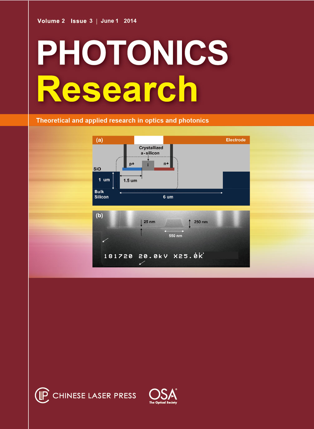
We present photonics technology based on a bulk-Si substrate for cost-sensitive dynamic random-access memory (DRAM) optical interface application. We summarize the progress on passive and active photonic devices using a local-crystallized Si waveguide fabricated by solid phase epitaxy or laser-induced epitaxial growth on bulk-Si substrate. The process of integration of a photonic integrated circuit (IC) with an electronic IC is demonstrated using a 65 nm DRAM periphery process on 300 mm wafers to prove the possibility of seamless integration with various complementary metal-oxide-semiconductor devices. Using the bulk-Si photonic devices, we show the feasibility of high-speed multidrop interface: the Mach–Zehnder interferometer modulators and commercial photodetectors are used to demonstrate four-drop link operation at 10 Gb/s, and the transceiver chips with photonic die and electronic die work for the DDR3 DRAM interface at 1.6 Gb/s under a 1∶4 multidrop configuration.
Hyunil Byun, Jinkwon Bok, Kwansik Cho, Keunyeong Cho, Hanmei Choi, Jinyong Choi, Sanghun Choi, Sangdeuk Han, Seokyong Hong, Seokhun Hyun, T. J. Jeong, Ho-Chul Ji, In-Sung Joe, Beomseok Kim, Donghyun Kim, Junghye Kim, Jeong-Kyoum Kim, Kiho Kim, Seong-Gu Kim, Duanhua Kong, Bongjin Kuh, Hyuckjoon Kwon, Beomsuk Lee, Hocheol Lee, Kwanghyun Lee, Shinyoung Lee, Kyoungwon Na, Jeongsik Nam, Amir Nejadmalayeri, Yongsang Park, Sunil Parmar, Junghyung Pyo, Dongjae Shin, Joonghan Shin, Yong-hwack Shin, Sung-Dong Suh, Honggoo Yoon, Yoondong Park, Junghwan Choi, Kyoung-Ho Ha, Gitae Jeong. Bulk-Si photonics technology for DRAM interface [Invited][J]. Photonics Research, 2014, 2(3): 03000A25.


 PDF全文
PDF全文

