Photonics Research, 2020, 8 (10): 10001648, Published Online: Sep. 30, 2020
56 Gbps high-speed Ge electro-absorption modulator  Download: 711次
Abstract
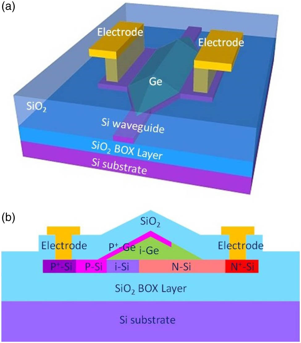
A high-speed evanescent-coupled Ge waveguide electro-absorption modulator (EAM) with simple fabrication processes was realized on a silicon-on-insulator platform with a 220 nm top Si layer. Selectively grown Ge with a triangle shape was directly used for Ge waveguides of the EAM. An asymmetric p-i-n junction was designed in the Ge waveguide to provide a strong electric field for Franz–Keldysh effect. The insertion loss of the Ge EAM was 6.2 dB at 1610 nm. The EAM showed the high electro-optic bandwidth of 36 GHz at
Zhi Liu, Xiuli Li, Chaoqun Niu, Jun Zheng, Chunlai Xue, Yuhua Zuo, Buwen Cheng. 56 Gbps high-speed Ge electro-absorption modulator[J]. Photonics Research, 2020, 8(10): 10001648.


