激光与光电子学进展, 2019, 56 (16): 163201, 网络出版: 2019-08-05
基于激光干涉烧蚀的硅表面微纳结构制备研究  下载: 1947次封面文章
Fabrication of Silicon Micro/Nanostructures Based on Laser Interference Ablation
超快光学 干涉烧蚀 纳秒激光 周期性微纳结构 周期劈裂 ultrafast optics interference ablation nanosecond laser periodic micro/nanostructures period splitting
")
摘要
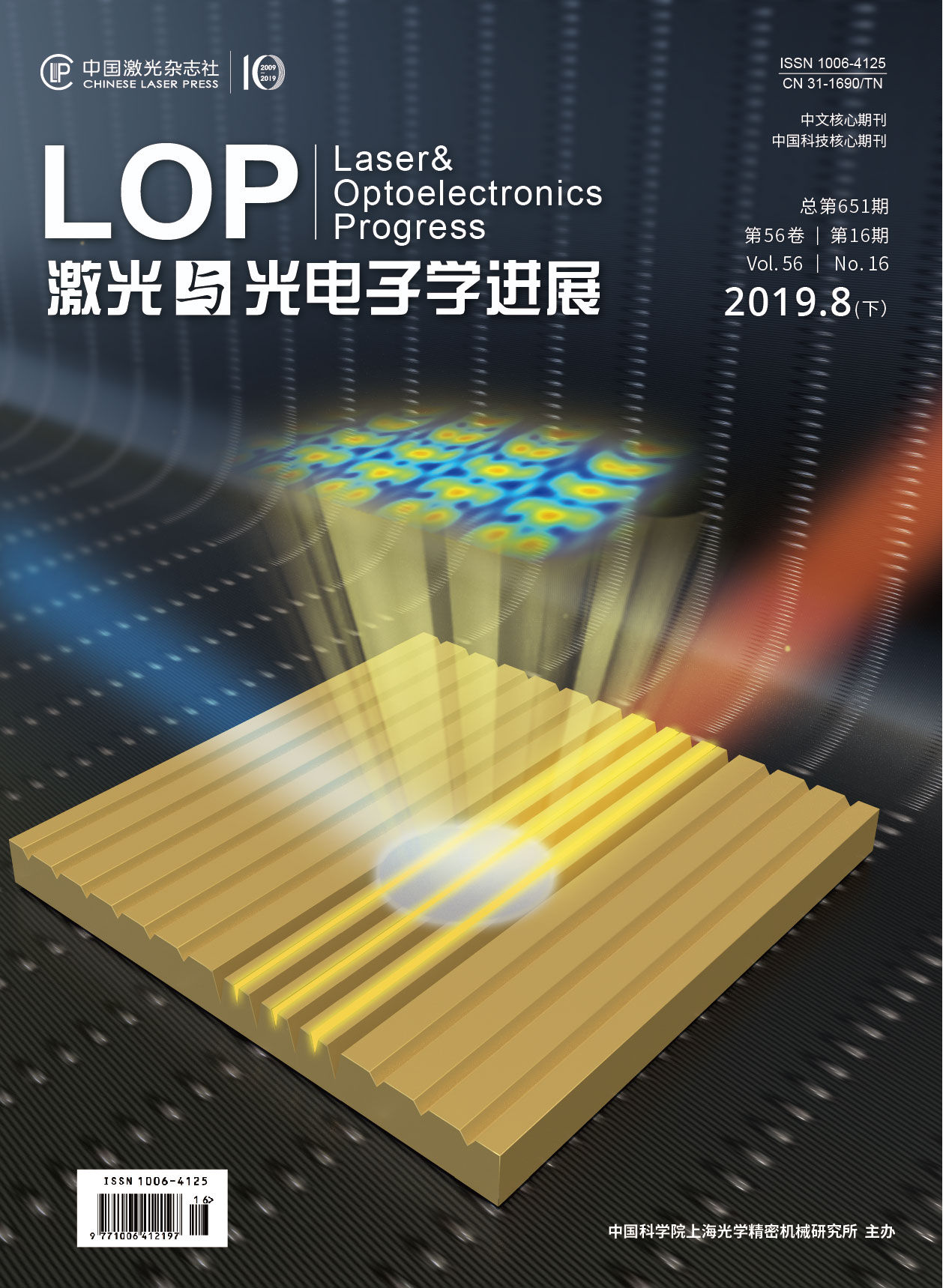
基于纳秒激光双光束干涉烧蚀技术,辅助利用湿法腐蚀技术,并结合时域有限差分法,从实验和理论上分析研究了硅表面不同周期微纳结构的制备和形成机制。结果表明:波长为355 nm的纳秒激光,可在硅表面干涉烧蚀出600 nm以上周期的微纳结构;结构深度随功率或曝光时间的增加而加深,最大深度可达到激光的趋肤深度约50 nm;结构周期在曝光时间大于5 s时发生劈裂减半,最小可以得到300 nm的周期;通过时域有限差分(FDTD)的理论模拟发现,已形成结构对干涉光场的调制是结构劈裂的最主要原因。这些研究将在表面周期性微纳结构的制备、无掩模快速加工设备的研制、以及激光与物质的相互作用等方面有很大的应用前景。
Abstract
Based on nanosecond laser two-beam interference ablation assisted with wet-etching method and finite difference time domain (FDTD) simulation, the formation of structures on silicon is studied experimentally and theoretically. The results show that it is possible for the fabrication of structures with period more than 600 nm by a nanosecond laser with wavelength of 355 nm. The structure depth becomes deeper with the increasing of power or exposure time. The maximum depth is equal to the skin depth of laser, about 50 nm. Further, the period splits into half when the exposure time is more than 5 s, which brings a method to obtain a minimum period of 300 nm. The FDTD simulation confirms that the modulation of formed structures to the interference field is the reason for period splitting. The research shows great potential applications for the fabrication of periodic micro/nanostructures, design of maskless processing facilities, and laser-matter interactions.
王子涵, 王宝续, 釜野勝, 徐微微. 基于激光干涉烧蚀的硅表面微纳结构制备研究[J]. 激光与光电子学进展, 2019, 56(16): 163201. Zihan Wang, Baoxu Wang, Masaru Kamano, Weiwei Xu. Fabrication of Silicon Micro/Nanostructures Based on Laser Interference Ablation[J]. Laser & Optoelectronics Progress, 2019, 56(16): 163201.


 PDF全文
PDF全文

