
2017, 5(5) Column
Photonics Research 第5卷 第5期

Enhanced magneto-optical Kerr effect and index sensitivity in Au/FexCo1-x magnetoplasmonic transducers Download:692次
Download:692次Magnetoplasmonic sensors are attractive candidates for ultrasensitive chemical and biomedical sensor applications. A variety of ferromagnetic metal thin films have been used for magnetoplasmonic device applications, yet the dependence of sensor performance on the optical and magneto-optical properties of ferromagnetic metal materials has been rarely studied. In this work, we report the study of enhanced magneto-optical Kerr effect (MOKE) and sensing performance in Au/FexCo1?x bilayer magneto-optical surface plasmon resonance (MOSPR) transducers. The optical constants of FexCo1?x (x=0, 0.29, 0.47, 0.65, and 1) in a sputter-deposited Au/FexCo1?x device are characterized by the attenuated total internal reflection (ATR) method. FexCo1?x thin films show different MOKEs as a function of the chemical concentration, with the highest transverse MOKE signal observed in Fe0.7Co0.3. Index sensing performance is closely related to the material’s optical and magneto-optical constants. By studying the sensing performance in the parameter space of the Au/FexCo1?x bilayer thicknesses, the highest sensitivity is found to be 0.385 (theoretical) and 0.306 RIU?1 (experimental) in the Au/Fe0.7Co0.3 MOSPR devices. Our research highlights the influence of the optical properties of ferromagnetic material to device sensitivity in MOSPR transducers. The high sensitivity in Au/FexCo1?x MOSPR devices make these structures attractive candidates for chemical and biomedical sensing applications.
(280.0280) Remote sensing and sensors (240.6680) Surface plasmons (160.3820) Magneto-optical materials. 

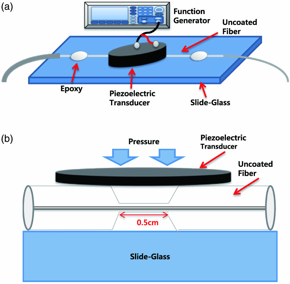
All-fiber acousto-optic modulator based on a cladding-etched optical fiber for active mode-lockingDownload:547次
Download:547次An all-fiber acousto-optic modulator (AOM), which features a compact structure and a low-driving voltage, is experimentally demonstrated for the active mode-locking of a fiber laser. The proposed AOM is based on the short length of the cladding-etched fiber, the ends of which are fixed on a slide glass. On top of the cladding-etched fiber, a piezoelectric transducer was overlaid. A chemical wet-etching technique, which is based on a mixed solution of NH4F and (NH4)2SO4, is used to reduce the fiber diameter down to ~25 μm, and the length of the etched section is only 0.5 cm. The fabricated device exhibited a modulation depth of 73.10% at an acoustic frequency of 918.9 kHz and a peak-to-peak electrical voltage of 10 V, while a laser beam was coupled at 1560 nm. By using the prepared AOM within an erbium-doped-fiber ring cavity, the mode-locked pulses with a temporal width of 2.66 ps were readily obtained at a repetition rate of 1.838 MHz.
(060.2340) Fiber optics components (140.4050) Mode-locked lasers (230.1040) Acousto-optical devices. 
Optical whispering gallery microcavities with high-quality factors have shown great potential toward achieveing ultrahigh-sensitivity sensing up to a single molecule or nanoparticle, which raises a huge demand on a deep theoretical insight into the crucial phenomena such as the mode shift, mode splitting, and mode broadening in sensing experiments. Here we propose an intuitive model to analyze these phenomena from the viewpoint of the nanoparticle-induced multiple scattering of the azimuthally propagating mode (APM). The model unveils explicit relations between these phenomena and the phase change and energy loss of the APM when scattered at the nanoparticle; the model also explains the observed polarization-dependent preservation of one resonance and the particle-dependent redshift or blueshift. The model indicates that the particle-induced coupling between the pair of unperturbed degenerate whispering gallery modes (WGMs) and the coupling between the WGMs and the free-space radiation modes, which are widely adopted in current theoretical formalisms, are realized via the reflection and scattering-induced free-space radiation of the APM, respectively, and additionally exhibits the contribution of cross coupling between the unperturbed WGMs and other different WGMs to forming the splitting resonant modes, especially for large particles.
(260.5740) Resonance (130.6010) Sensors (290.5850) Scattering particles (290.4210) Multiple scattering. 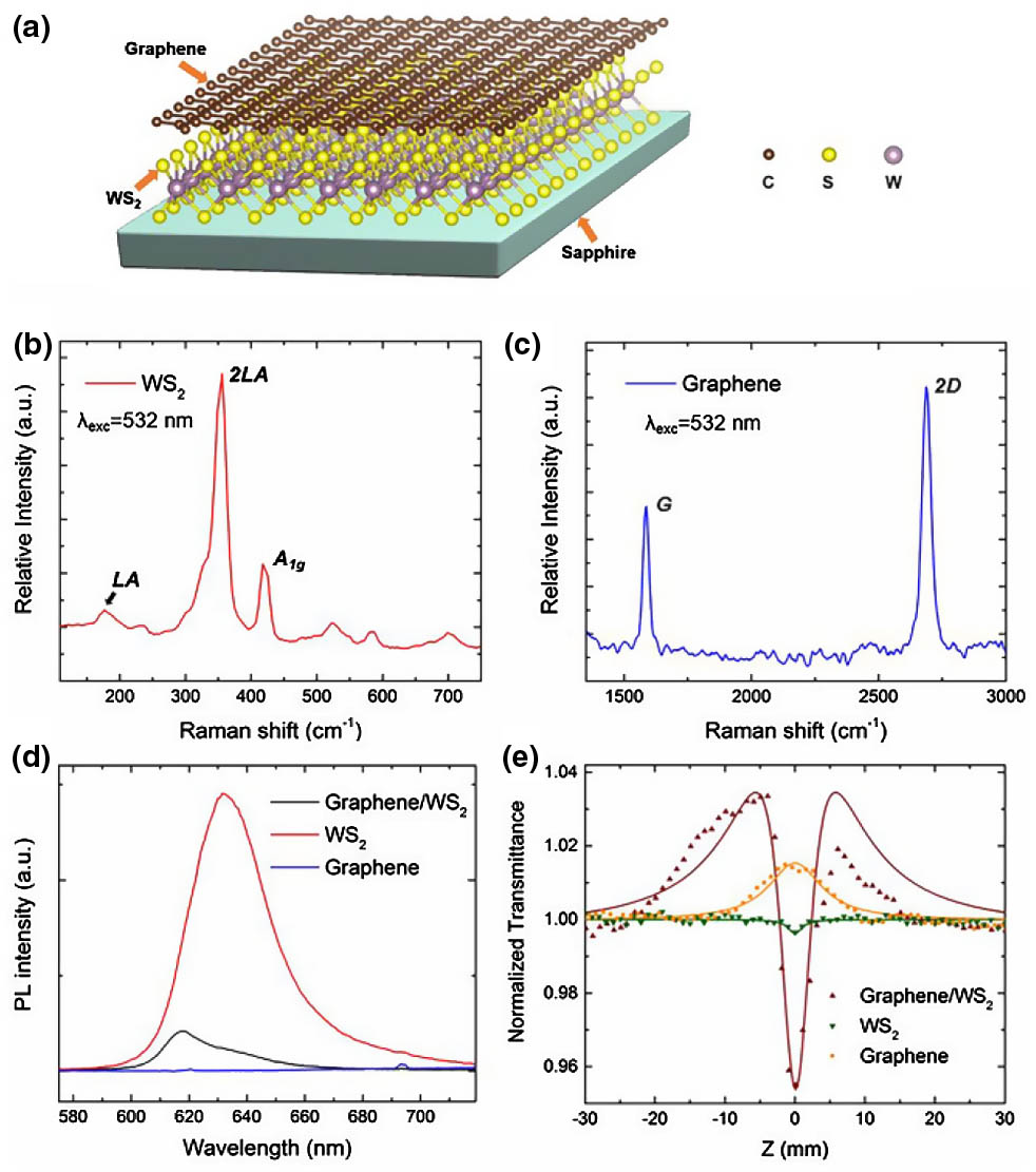
We report on the operation of passively Q-switched waveguide lasers at 1 μm wavelength based on a graphene/WS2 heterostructure as a saturable absorber (SA). The gain medium is a crystalline Nd:YVO4 cladding waveguide produced by femtosecond laser writing. The nanosecond waveguide laser operation at 1064 nm has been realized with the maximum average output power of 275 mW and slope efficiency of 37%. In comparison with the systems based on single WS2 or graphene SA, the lasing Q-switched by a graphene/WS2 heterostructure SA possesses advantages of a higher pulse energy and enhanced slope efficiency, indicating the promising applications of van der Waals heterostructures for ultrafast photonic devices.
(230.7370) Waveguides (140.3540) Lasers Q-switched (130.0130) Integrated optics (160.4236) Nanomaterials. 
In this study, a full-color emission red–green–blue (RGB) quantum-dot (QD)-based micro-light-emitting-diode (micro-LED) array with the reduced optical cross-talk effect by a photoresist mold has been demonstrated. The UV micro-LED array is used as an efficient excitation source for the QDs. The aerosol jet technique provides a narrow linewidth on the micrometer scale for a precise jet of QDs on the micro-LEDs. To reduce the optical cross-talk effect, a simple lithography method and photoresist are used to fabricate the mold, which consists of a window for QD jetting and a blocking wall for cross-talk reduction. The cross-talk effect of the well-confined QDs in the window is confirmed by a fluorescence microscope, which shows clear separation between QD pixels. A distributed Bragg reflector is covered on the micro-LED array and the QDs’ jetted mold to further increase the reuse of UV light. The enhanced light emission of the QDs is 5%, 32%, and 23% for blue, green, and red QDs, respectively.
(120.2040) Displays (160.4236) Nanomaterials (230.2090) Electro-optical devices (230.3670) Light-emitting diodes. 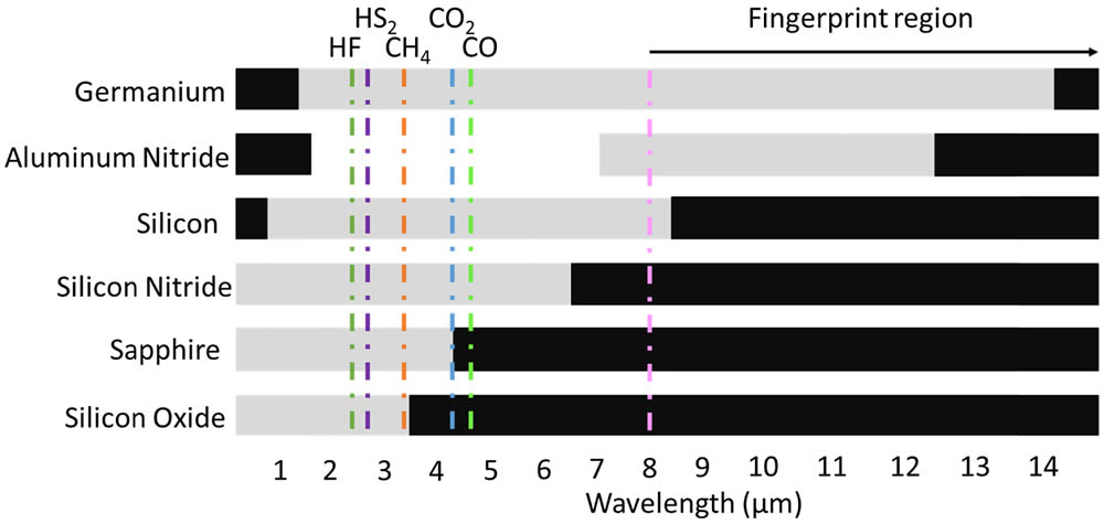
Silicon photonic integrated circuits for telecommunication and data centers have been well studied in the past decade, and now most related efforts have been progressing toward commercialization. Scaling up the silicon-on-insulator (SOI)-based device dimensions in order to extend the operation wavelength to the short mid-infrared (MIR) range (2–4 μm) is attracting research interest, owing to the host of potential applications in lab-on-chip sensors, free space communications, and much more. Other material systems and technology platforms, including silicon-on-silicon nitride, germanium-on-silicon, germanium-on-SOI, germanium-on-silicon nitride, sapphire-on-silicon, SiGe alloy-on-silicon, and aluminum nitride-on-insulator are explored as well in order to realize low-loss waveguide devices for different MIR wavelengths. In this paper, we will comprehensively review silicon photonics for MIR applications, with regard to the state-of-the-art achievements from various device demonstrations in different material platforms by various groups. We will then introduce in detail of our institute’s research and development efforts on the MIR photonic platforms as one case study. Meanwhile, we will discuss the integration schemes along with remaining challenges in devices (e.g., light source) and integration. A few application-oriented examples will be examined to illustrate the issues needing a critical solution toward the final production path (e.g., gas sensors). Finally, we will provide our assessment of the outlook of potential future research topics and engineering challenges along with opportunities.
(130.0130) Integrated optics (130.3120) Integrated optics devices (130.6622) Subsystem integration and techniques. 
The effect of background light on the imaging quality of three typical ghost imaging (GI) lidar systems (namely narrow pulsed GI lidar, heterodyne GI lidar, and pulse-compression GI lidar via coherent detection) is investigated. By computing the signal-to-noise ratio (SNR) of fluctuation-correlation GI, our analytical results, which are backed up by numerical simulations, demonstrate that pulse-compression GI lidar via coherent detection has the strongest capacity against background light, whereas the reconstruction quality of narrow pulsed GI lidar is the most vulnerable to background light. The relationship between the peak SNR of the reconstruction image and σ (namely, the signal power to background power ratio) for the three GI lidar systems is also presented, and the results accord with the curve of SNR-σ.
(110.0110) Imaging systems (110.2990) Image formation theory (110.1758) Computational imaging. 
We theoretically propose blue-detuned optical trapping for neutral atoms via strong near-field interfacing in a plasmonic nanohole array. The optical field at resonance forms a nanoscale-trap potential with an FWHM of 200 nm and about ~370 nm away from the nanohole; thus, a stable 3D atom trapping independent of the surface potential is demonstrated. The effective trap depth is more than 1 mK when the optical power of trapping light is only about 0.5 mW, while the atom scattering rate is merely about 3.31 s?1, and the trap lifetime is about 800 s. This compact plasmonic structure provides high uniformity of trap depths and a two-layer array of atom nanotraps, which should have important applications in the manipulation of cold atoms and collective resonance fluorescence.
(240.6680) Surface plasmons (230.4555) Coupled resonators (020.1335) Atom optics (020.7010) Laser trapping. 
Control of chirality using metamaterials plays a critical role in a diverse set of advanced photonics applications, such as polarization control, bio-sensing, and polarization-sensitive imaging devices. However, this poses a major challenge, as it primarily involves the geometrical reconfiguration of metamolecules that cannot be adjusted dynamically. Real-world applications require active tuning of the chirality, which can easily manipulate the magnitude, handedness, and spectral range of chiroptical response. Here, enabled by graphene, we theoretically reveal a tunable/switchable achiral metasurface in the near-infrared region. In the model, the achiral metasurface consists of an array of circular holes embedded through a metal/dielectric/metal trilayer incorporated with the graphene sheet, where holes occupy the sites of a rectangular lattice. Circular conversion dichroism (CCD) originates from the mutual orientation between the achiral metasurface and oblique incident wave. The achiral metasurface possesses dual-band sharp features in the CCD spectra, which are tuned over a broad bandwidth by electrically modulating the graphene’s Fermi level. By selecting aluminium as the metal materials, we numerically achieved strong CCD and considerably reduced materials costs with our nanostructures compared with the typically used noble metals such as gold and silver.
(160.3918) Metamaterials (160.1585) Chiral media (240.6680) Surface plasmons. 
Cavity optomechanics is applied to study the coupling behavior of interacting molecules in surface plasmon systems driven by two-color laser beams. Different from the traditional force–distance measurement, due to a resonant frequency shift or a peak splitting on the probe spectrum, we have proposed a convenient method to measure the van der Waals force strength and interaction energy via nonlinear spectroscopy. The minimum force value can reach approximately 10?15 N, which is 3 to 4 orders of magnitude smaller than the widely applied atomic force microscope (AFM). It is also shown that two adjacent molecules with similar chemical structures and nearly equal vibrational frequencies can be easily distinguished by the splitting of the transparency peak. Based on this coupled optomechanical system, we also conceptually design a tunable optical switch by van der Waals interaction. Our results will provide new approaches for understanding the complex and dynamic interactions in molecule–plasmon systems.
(120.4880) Optomechanics (240.6680) Surface plasmons (300.6290) Spectroscopy four-wave mixing (300.6390) Spectroscopy molecular. 
CsPbBr3 perovskite quantum dots: saturable absorption properties and passively Q-switched visible lasersDownload:1108次
Download:1108次This work presents the saturable absorption (SA) properties of CsPbBr3 perovskite quantum dots (QDs). The perovskite QDs show excellent SA performance with a nonlinear absorption coefficient of ?35×10?2 cm/GW and a figure of merit of 3.7×10?14 esu?cm. Further, their use as saturable absorbers in a passively Q-switched visible solid-state laser for the generation of soliton pulses is demonstrated. These results demonstrate the potential for the perovskite QDs to act as saturable absorbers.
(190.4400) Nonlinear optics materials (160.4670) Optical materials (160.4760) Optical properties. 
High-power passively Q-switched 2 μm all-solid-state laser based on a Bi2Te3 saturable absorberDownload:788次
Download:788次By using the ultrasound-assisted liquid phase exfoliation method, Bi2Te3 nanosheets are synthesized and deposited onto a quartz plate to form a kind of saturable absorber (SA), in which nonlinear absorption properties around 2 μm are analyzed with a home-made mode-locked laser. With the as-prepared Bi2Te3 SA employed, a stable passively Q-switched all-solid-state 2 μm laser is successfully realized. Q-switched pulses with a maximum average output power of 2.03 W are generated under an output coupling of 5%, corresponding to the maximum single-pulse energy of 18.4 μJ and peak power of 23 W. The delivered shortest pulse duration and maximum repetition rate are 620 ns and 118 kHz under an output coupling of 2%, respectively. It is the first presentation of such Bi2Te3 SA employed in a solid-state Q-switched crystalline laser at 2 μm, to the best of our knowledge. In comparison with other 2D materials suitable for pulsed 2 μm lasers, the saturable absorption performance of Bi2Te3 SA is proved to be promising in generating high power and high-repetition-rate 2 μm laser pulses.
(140.3070) Infrared and far-infrared lasers (140.3580) Lasers solid-state (140.3540) Lasers Q-switched (160.4330) Nonlinear optical materials (160.4236) Nanomaterials. 
Enhanced spin Hall effect of reflected light with guided-wave surface plasmon resonanceDownload:666次
Download:666次The photonic spin Hall effect (SHE) has been intensively studied and widely applied, especially in spin photonics. However, the SHE is weak and is difficult to detect directly. In this paper, we propose a method to enhance SHE with the guided-wave surface-plasmon resonance (SPR). By covering a dielectric with high refractive index on the surface of silver film, the photonic SHE can be greatly enhanced, and a giant transverse shift of horizontal polarization state is observed due to the evanescent field enhancement near the interface at the top dielectric layer and air. The maximum transverse shift of the horizontal polarization state with 11.5 μm is obtained when the thickness of Si film is optimum. There is at least an order of magnitude enhancement in contrast with the transverse shift in the conventional SPR configuration. Our research is important for providing an effective way to improve the photonic SHE and may offer the opportunity to characterize the parameters of the dielectric layer with the help of weak measurements and development of sensors based on the photonic SHE.
(240.0240) Optics at surfaces (260.6970) Total internal reflection (310.2785) Guided wave applications. 
Tunable luminescent CsPb2Br5 nanoplatelets: applications in light-emitting diodes and photodetectorsDownload:1284次
Download:1284次Unlike organic–inorganic hybrid perovskites, all-inorganic cesium lead halide perovskites hold great promise for developing high-performance optoelectronic devices, owing to their improved stability. Herein, we investigate the perovskite-related CsPb2Br5 nanoplatelets (NPLs) with tunable emission wavelengths via changing the reaction temperatures to 100°C, 120°C, and 140°C. Reaction temperature plays a key role in determining the shapes and thicknesses of the resulting CsPb2Br5 NPLs. A higher temperature is in favor of the formation of smaller and thicker NPLs. To develop their potential applications in optoelectronic devices, green light emitting diodes (LEDs) and photodetectors based on CsPb2Br5 NPLs are fabricated. The green LEDs based on CsPb2Br5 NPLs synthesized at 140°C exhibit an excellent pure green emission (full width at half-maximum of <20 nm) and display a luminous efficiency of 34.49 lm/W under an operation current of 10 mA. Moreover, the photodetector based on CsPb2Br5 NPLs synthesized at 100°C has better performance with a rise time of 0.426 s, a decay time of 0.422 s, and a ratio of the current (with and without irradiation) of 364%.
(160.4236) Nanomaterials (160.4670) Optical materials (230.3670) Light-emitting diodes (040.5160) Photodetectors. 
The ability to modulate an optical field via an electric field is regarded as a key function of electro-optic interconnects, which are used in optical communications and information-processing systems. One of the main devices required for such interconnects is the electro-optic modulator (EOM). Current EOMs based on the electro-optic and electro-absorption effects often are bulky and power-inefficient due to the weak electro-optic properties of their constituent materials. Here, we propose a new mechanism to produce an arbitrary-waveform EOM based on quantum interference, in which both the real and imaginary parts of the susceptibility are engineered coherently with super-high efficiency. Based on this EOM, a waveform interconnect from the voltage to the modulated optical absorption is realized. We expect that such a new type of electro-optic interconnect will have a broad range of applications, including in optical communications and networks.
(250.4110) Modulators (200.4650) Optical interconnects (270.5580) Quantum electrodynamics (250.5300) Photonic integrated circuits. 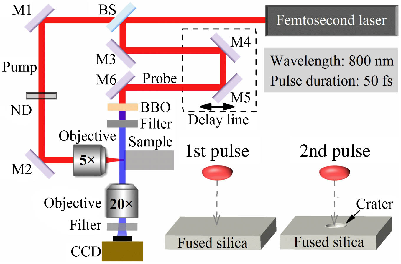
The dynamics of plasma and shockwave expansion during two femtosecond laser pulse ablation of fused silica are studied using a time-resolved shadowgraph imaging technique. The experimental results reveal that during the second pulse irradiation on the crater induced by the first pulse, the expansion of the plasma and shockwave is enhanced in the longitudinal direction. The plasma model and Fresnel diffraction theory are combined to calculate the laser intensity distribution by considering the change in surface morphology and transient material properties. The theoretical results show that after the free electron density induced by the rising edge of the pulse reaches the critical density, the originally transparent surface is transformed into a transient high-reflectivity surface (metallic state). Thus, the crater with a concave-lens-like morphology can tremendously reflect and refocus the latter part of the laser pulse, leading to a strong laser field with an intensity even higher than the incident intensity. This strong refocused laser pulse results in a stronger laser-induced air breakdown and enhances the subsequent expansion of the plasma and shockwave. In addition, similar shadowgraphs are also recorded in the single-pulse ablation of a concave microlens, providing experimental evidence for the enhancement mechanism.
(320.7100) Ultrafast measurements (140.3390) Laser materials processing (140.3440) Laser-induced breakdown. 
We experimentally demonstrate the optical properties of gratings engraved in a single-mode waveguide fabricated on top of a dielectric multilayer platform. The structure can be approached as a reflector for Bloch-surface-wave-based two-dimensional optical systems. The gratings have been fabricated on a thin (~λ/25) titanium dioxide layer with a thickness of a few tens of nanometers deposited on the top of a multilayer platform. The optical properties of the gratings have been characterized in the near field with the aid of multi-heterodyne scanning near-field optical microscopy. We investigate the surface wave’s interference pattern, produced by incident and reflected light in front of the gratings. The presented gratings behave as an efficient Bloch-surface–wave-based reflector at telecommunication wavelength.
(240.0240) Optics at surfaces (240.6690) Surface waves. 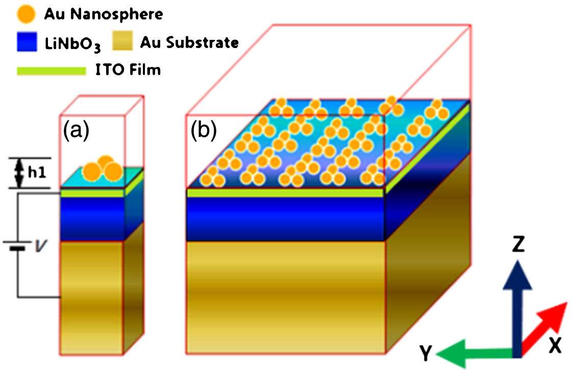
A narrowband tunable antireflection optical filter is proposed and numerically studied. The structure is a metasurface based on plasmonic nanoparticles on an electro-optic film in a three-layer configuration of metal-dielectric-metal (MDM) in the visible near-infrared range. By tuning the voltage and thus tuning the refractive index of the dielectric LiNbO3, one can shift the wavelength of minimum reflection as desired. The parameters of gold nanoparticles and other elements used for the filter design and refractive index of the dielectric are obtained by the finite-element method (FEM). An analytical theory is presented to explain the FEM simulation results, and they agree well with each other. It is found that the frequency of the plasmonic resonance wave on the metasurface should be equal to that of the Fabry–Perot resonator formed by the MDM to have a good filtering property. Theoretical spectra obtained by FEM simulation show that the structure has extensive potential for the design of tunable narrow-band filters for modulators, displayers, and color extraction for imaging.
(120.2440) Filters (230.2090) Electro-optical devices (240.6680) Surface plasmons (160.3918) Metamaterials. A few-mode (FM) vertical cavity surface emitting laser (VCSEL) chip with heavily zinc-diffused contact layer and oxide-confined cross-section is demonstrated for carrying pre-leveled 16-quadrature amplitude modulation orthogonal frequency division multiplexing (QAM-OFDM) data in OM4 multi-mode fiber (MMF) over 100 m for intra-data-center applications. The FM VCSEL chip, which has an oxide-confined emission aperture of 5 μm, demonstrates high external quantum efficiency, provides an optical power of 2.2 mW at 38 times threshold condition, and exhibits 3 dB direct-modulation bandwidth beyond 22 GHz at a cost of slight heat accumulation. At a DC bias point of 5 mA (22.6Ith) the FM VCSEL chip, with sufficiently normalized modulation output, supports Baud and data rates of 25 and 100 Gb/s, respectively, with forward error correction (FEC) certifying receiving quality after back-to-back transmission. After passing through 100 m OM4 MMF with a receiving power penalty of 4 dB, the FM VCSEL chip demonstrates FEC-certified transmission of the pre-leveled 16-QAM OFDM data at 92 Gb/s.
Vertical cavity surface emitting lasers Fiber optics infrared Optical interconnects 
Theoretical aspects and sensing demonstrations of cone-shaped inwall capillary-based microsphere resonatorsDownload:745次
Download:745次In this paper, a detailed theoretical study on the characteristics of cone-shaped inwall capillary-based microsphere resonators is described and demonstrated for sensing applications. The maximum, minimum, slope, contrast, and width of the Fano resonance are analyzed. As the transmission coefficient of the capillary resonator increases, the absolute value of the slope of Fano resonances increases to reach its maximum, which is useful for sensors with an ultra-high sensitivity. There occurs another phenomenon of electromagnetically induced transparency when the reflectivity at the capillary–environment interface is close to 100%. We also experimentally demonstrated its capability for temperature and refractive index sensing, with a sensitivity of 10.9 pm/°C and 431 dB/RIU based on the Fano resonance and the Lorentzian line shape, respectively.
(230.5750) Resonators (060.2370) Fiber optics sensors. 
On-chip silicon photonic 2 × 2 mode- and polarization-selective switch with low inter-modal crosstalkDownload:681次
Download:681次Mode- and polarization-division multiplexing offer new dimensions to increase the transmission capacity of optical communications. Selective switches are key components in reconfigurable optical network nodes. An on-chip silicon 2×2 mode- and polarization-selective switch that can route four data channels on two modes and two polarizations simultaneously is proposed and experimentally demonstrated for the first time, to the best of our knowledge. The overall insertion losses are lower than 8.6 dB. To reduce the inter-modal crosstalk, polarization beam splitters are added to filter the undesired polarizations or modes. The measured inter-modal and intra-modal crosstalk values are below ?23.2 and ?22.8 dB for all the channels, respectively.
(130.3120) Integrated optics devices (060.4230) Multiplexing (130.4815) Optical switching devices. 
Coupling efficiency between the localized surface plasmons (LSPs) of metal nanoparticles (NPs) and incident light dominates the sensitivities of plasmon-based sensing spectroscopies and imaging techniques, e.g., surface-enhanced Raman scattering (SERS) spectroscopy. Many endogenous features of metal NPs (e.g., size, shape, aggregation form, etc.) that have strong impacts on their LSPs have been discussed in detail in previous studies. Here, the polarization-tuned electromagnetic (EM) field that facilitates the LSP coupling is fully discussed. Numerical analyses on waveguide-based evanescent fields (WEFs) coupled with the LSPs of dispersed silver nanospheres and silver nano-hemispheres are presented and the applicability of the WEF-LSPs to plasmon-enhanced spectroscopy is discussed. Compared with LSPs under direct light excitation that only provide 3–4 times enhancement of the incidence field, the WEF-LSPs can amplify the electric field intensity about 30–90 times (equaling the enhancement factor of 106–108 in SERS intensity), which is comparable to the EM amplification of the SERS “hot spot” effect. Importantly, the strongest region of EM enhancement around silver nanospheres can be modulated from the gap region to the side surface simply by switching the incident polarization from TM to TE, which widely extends its sensing applications in surface analysis of monolayer of molecule and macromolecule detections. This technique provides us a unique way to achieve remarkable signal gains in many plasmon-enhanced spectroscopic systems in which LSPs are involved.
(300.0300) Spectroscopy (300.6390) Spectroscopy molecular (300.6450) Spectroscopy Raman (300.6490) Spectroscopy surface. 
影响因子:7.6
CN:31-2126/O4
ISSN:2327-9125


公告
动态信息
动态信息 丨 2024-04-11
PR Highlight (Vol. 11, Iss. 12): 亮点 | 十亿像素级、高通量的无透镜偏振编码叠层成像技术动态信息 丨 2024-03-29
PR 封面故事 (Vol. 12, Iss. 3): 封面 | 基于时空编码神经网络的像差感知超分辨成像动态信息 丨 2024-03-25
PR 封面故事 (Vol. 12, Iss. 1) 光涡旋与手性器件微纳3D打印动态信息 丨 2024-03-14
PR Highlight (Vol. 12, Iss. 1): 同步双脉冲激光烧蚀中的气泡相互作用效应动态信息 丨 2024-03-04
PR Highlight (Vol. 11, Iss. 12): 利用钙钛矿微米线异质结构,实现高性能偏振敏感光电探测激光评论微信公众号

点击菜单“联系编辑”即可添加期刊编辑为好友啦