2018, 6(9) Column
Photonics Research 第6卷 第9期
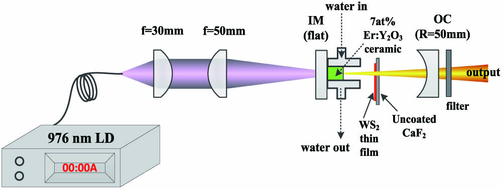
We report on diode-pumped Er : Y 2 O 3 Q WS 2 Q Q WS 2 Q Er : Y 2 O 3 Q
Lasers, diode-pumped Lasers, Q-switched Lasers, solid-state Computer-generated holography (CGH) is a technique for converting a three-dimensional (3D) object scene into a two-dimensional (2D), complex-valued hologram. One of the major bottlenecks of CGH is the intensive computation that is involved in the hologram generation process. To overcome this problem, numerous research works have been conducted with the aim of reducing arithmetic operations involved in CGH. In this paper, we shall review a number of fast CGH methods that have been developed in the past decade. These methods, which are commonly referred to as point-based CGH, are applied to compute digital Fresnel holograms for an object space that is represented in a point cloud model. While each method has its own strength and weakness, trading off conflicting issues, such as computation efficiency and memory requirement, they also exhibit potential grounds of synergy. We hope that this paper will bring out the essence of each method and provide some insight on how different methods may crossover into better ones.
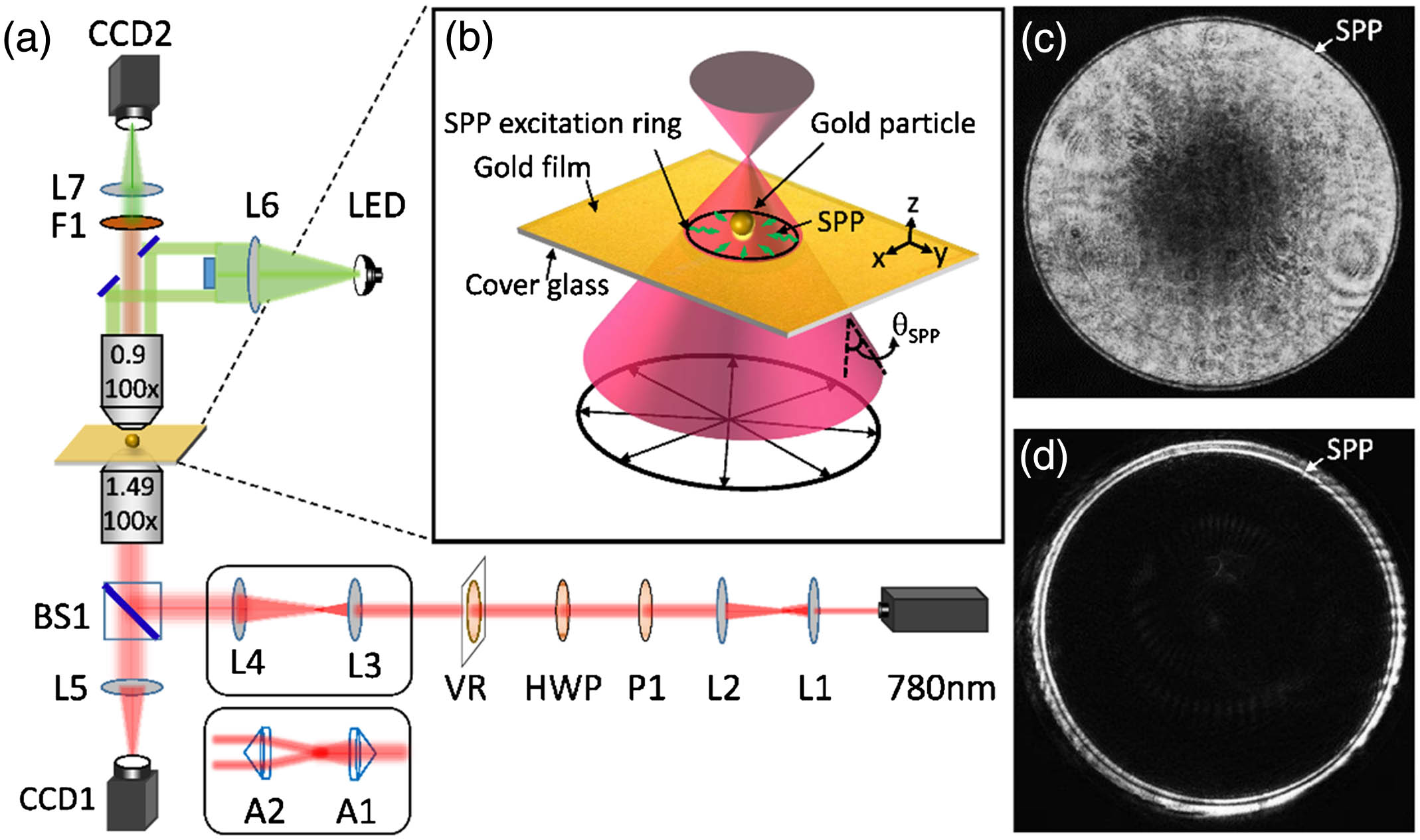
Computer holography Digital holography Strong plasmonic focal spots, excited by radially polarized light on a smooth thin metallic film, have been widely applied to trap various micro- and nano-sized objects. However, the direct transmission part of the incident light leads to the scattering force exerted on trapped particles, which seriously affects the stability of the plasmonic trap. Here we employ a novel perfect radially polarized beam to solve this problem. Both theoretical and experimental results verify that such a beam could strongly suppress the directly transmitted light to reduce the piconewton scattering force, and an enhanced plasmonic trapping stiffness that is 2.6 times higher is achieved in experiments. The present work opens up new opportunities for a variety of research requiring the stable manipulations of particles.
Polarization Optical tweezers or optical manipulation Plasmonics Mode-locked fiber lasers that can simultaneously generate two asynchronous ultrashort pulse trains could play an attractive role as the alternative light sources for low-complexity dual-comb metrology applications. Although a few multiplexing schemes to realize such lasers have been proposed and demonstrated, here we investigate the lasing characteristics of a passively mode-locked fiber laser with a finite amount of intracavity birefringence. By introducing a section of polarization-maintaining (PM) fiber into the otherwise-non-PM-single-mode cavity, dual asynchronous pulses with nearly orthogonal states of polarization are generated. With a repetition rate difference of hundreds of hertz, the pulses have well-overlapped spectra and show typical features of polarization-locked vector solitons. It is demonstrated that under an anomalous or net normal dispersion regime, either dual vector solitons or dual dissipative vector solitons can be generated, respectively. Such polarization-multiplexed single single-cavity dual-comb lasers could find further uses in various applications in need of simple dual-comb system solutions.
Mode-locked lasers Ultrafast lasers Lasers, fiber Heterogeneously integrating III-V materials on silicon photonic integrated circuits has emerged as a promising approach to make advanced laser sources for optical communication and sensing applications. Tunable semiconductor lasers operating in the 2–2.5 μm range are of great interest for industrial and medical applications since many gases (e.g., CO 2 CH 4
Integrated optics devices Lasers, tunable Lasers, ring Optical sensing and sensors Room temperature optical mass sensor with an artificial molecular structure based on surface plasmon optomechanics Download:654次
 Download:654次
We propose an optical weighing technique with a sensitivity down to a single atom through the coupling between a surface plasmon and a suspended graphene nanoribbon resonator. The mass is determined via the vibrational frequency shift on the probe absorption spectrum while the atom attaches to the nanoribbon surface. We provide methods to separate out the signals of the ultralow frequency vibrational modes from the strong Rayleigh background, first based on the quantum coupling with a pump-probe scheme. Owing to the spectral enhancement in the surface plasmon and the ultralight mass of the nanoribbon, this scheme results in a narrow linewidth (~ GHz ~ 30 yg
Optomechanics Surface plasmons Nanophotonics and photonic crystals Spectroscopy, atomic We investigate the properties of spatial solitons in the fractional Schr dinger equation (FSE) with parity-time (PT)-symmetric lattice potential supported by the focusing of Kerr nonlinearity. Both one- and two-dimensional solitons can stably propagate in PT-symmetric lattices under noise perturbations. The domains of stability for both one- and two-dimensional solitons strongly depend on the gain/loss strength of the lattice. In the spatial domain, the solitons are rigidly modulated by the lattice potential for the weak diffraction in FSE systems. In the inverse space, due to the periodicity of lattices, the spectra of solitons experience sharp peaks when the values of wavenumbers are even. The transverse power flows induced by the imaginary part of the lattice are also investigated, which can preserve the internal energy balances within the solitons.
Spatial solitons Fractional Fourier transforms Kerr effect Tunable optical delay lines are one of the key building blocks in optical communication and microwave systems. In this work, tunable optical delay lines based on integrated grating-assisted contradirectional couplers are proposed and experimentally demonstrated. The device performance is comprehensively improved in terms of parameter optimization, apodization analysis, and electrode design. Tunable group delay lines of 50 ps at different wavelengths within the bandwidth of 12 nm are realized with a grating length of 1.8 mm. Under thermal tuning mode, the actual delay tuning range is around 20 ps at 7.2 V voltage. At last, a new scheme adopting an ultra-compact reflector for doubling group delay is proposed and verified, achieving a large group delay line of 400 ps and a large dispersion value up to 5.5 × 10 6 ps / ( nm · km )
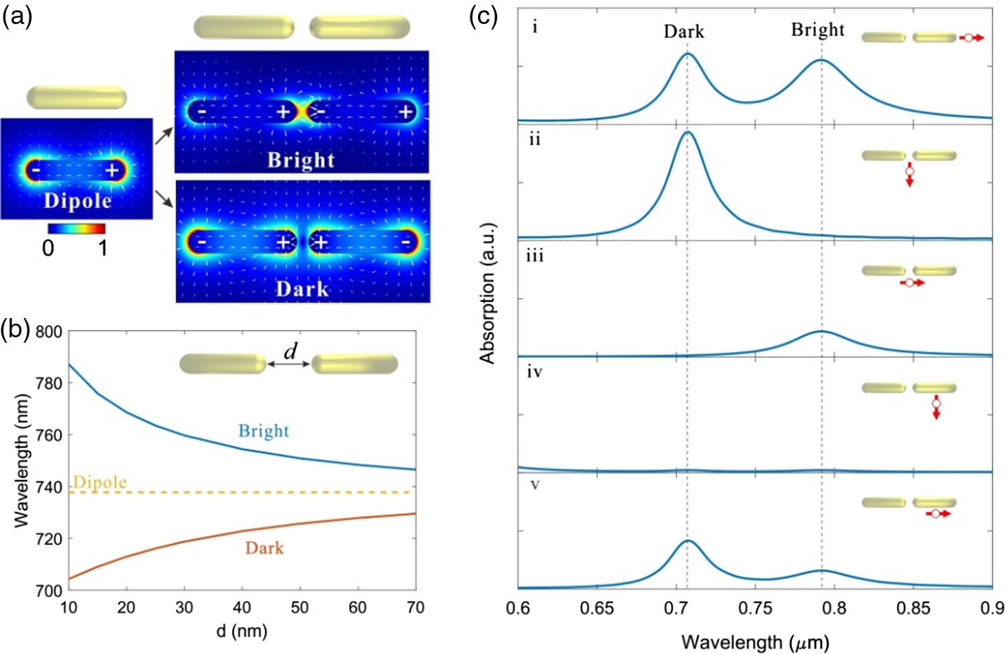
Integrated optics devices Wavelength filtering devices Optical buffers We theoretically investigate dark dimer mode excitation and strong coupling with a nanorod dipole. Efficient excitation of a dark mode in a gold (Au) nanorod dimer using an electric dipole can be achieved by an optimal overlap between the dipole moment and dark modal field. By replacing the dipole emitter with an Au nanorod, a plane wave excited dipole mode in the nanorod can be effectively coupled to the dark dimer mode through near-field interaction. At a 10-nm separation of the nanorod and the dimer, plasmonic interaction between dipole-dark modes enters the strong coupling regime with a Rabi-like splitting of 219.2 meV, which is further evidenced by the anticrossing feature and Rabi-like oscillation of electromagnetic energy of the coupled modes. Our results propose an efficient approach to far-field activating dark modes in coupled nanorod dimers and exchanging plasmonic excitations at nanoscale, which may open new opportunities for nanoplasmonic applications such as nanolasers or nanosensors.
Plasmonics Coupled resonators Surface plasmons We report a passively Q PtSe 2 Q Q PtSe 2 Q Q PtSe 2
Lasers, fiber Ultrafast lasers Laser materials Optical materials We experimentally demonstrate a long-term stable two-dimensional saturable absorption material under ambient conditions—multi-layer antimonene feasible for the mid-infrared spectral region—for the first time to our knowledge. The multi-layer antimonene material prepared using a liquid-phase exfoliation method was coated on a quartz/CaF 2 0.26 GW / cm 2 Ho 3 + / Pr 3 + Q
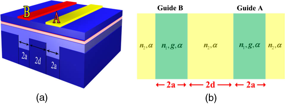
Infrared and far-infrared lasers Lasers, fiber Lasers, Q-switched Nanomaterials We study modulation properties of two-element phased-array semiconductor lasers that can be described by coupled mode theory. We consider four different waveguide structures and modulate the array either in phase or out of phase within the phase-locked regions, guided by stability diagrams obtained from direct numerical simulations. Specifically, we find that out-of-phase modulation allows for bandwidth enhancement if the waveguide structure is properly chosen; for example, for a combination of index antiguiding and gain-guiding, the achievable modulation bandwidth in the case of out-of-phase modulation could be much higher than the one when they are modulated in phase. Proper array design of the coupling, controllable in terms of the laser separation and the frequency offset between the two lasers, is shown to be beneficial to slightly improve the bandwidth but not the resonance frequency, while the inclusion of the frequency offset leads to the appearance of double peak response curves. For comparison, we explore the case of modulating only one element of the phased array and find that double peak response curves are found. To improve the resonance frequency and the modulation bandwidth, we introduce simultaneous external injection into the phased array and modulate the phased array or its master light within the injection locking region. We observe a significant improvement of the modulation properties, and in some cases, by modulating the amplitude of the master light before injection, the resulting 3 dB bandwidths could be enhanced up to 160 GHz. Such a record bandwidth for phased-array modulation could pave the way for various applications, notably optical communications that require high-speed integrated photonic devices.
Modulation Semiconductor lasers Laser arrays Waveguides, slab The denaturation of double-stranded deoxyribonucleic acid (ds-DNA) has been well known to break nucleobase bonds, resulting in single-stranded deoxyribonucleic acid (ss-DNA) in solutions, which can recombine to form ds-DNA in a reversible manner. We developed an efficient process to irreversibly maintain various DNA denaturation levels in thin solid films in order to investigate the impacts of the denaturation on the optical properties of DNA films. By adding NaOH in an aqueous solution of salmon testis DNA, we flexibly controlled the level of denaturation in the solution, which was then spin-coated on Si and silica substrates to irreversibly bind ss-DNAs in a thin solid film. The denaturation of DNA in thin solid films was experimentally confirmed by ultraviolet-visible and Fourier transform infrared spectroscopic investigations, whose level could be controlled by the NaOH content in the aqueous solution precursor. By this irreversible denaturation process, we developed a new method to flexibly vary the refractive index of DNA thin solid films in a wide range of Δ n > 0.02 n /dT of the films were also experimentally measured in the temperature range from 40°C to 90°C to confirm the significant impacts of denaturation. Detailed thin film processes and optical characterizations are discussed.
Biology Spectroscopy, ultraviolet Thin films, optical properties Mid-infrared (MIR) integrated photonics has attracted broad interest due to its promising applications in biochemical sensing, environmental monitoring, disease diagnosis, and optical communication. Among MIR integration platforms, germanium-based platforms hold many excellent properties, such as wide transparency windows, high refractive indices, and high nonlinear coefficients; however, the development of MIR germanium photonic devices is still in its infancy. Specifically, MIR high-Q Q ~ 18,000 Q
Infrared Integrated optics materials Photonic crystals Integrated optics devices 公告
动态信息
动态信息 丨 2024-04-11
PR Highlight (Vol. 11, Iss. 12): 亮点 | 十亿像素级、高通量的无透镜偏振编码叠层成像技术动态信息 丨 2024-03-29
PR 封面故事 (Vol. 12, Iss. 3): 封面 | 基于时空编码神经网络的像差感知超分辨成像动态信息 丨 2024-03-25
PR 封面故事 (Vol. 12, Iss. 1) 光涡旋与手性器件微纳3D打印动态信息 丨 2024-03-14
PR Highlight (Vol. 12, Iss. 1): 同步双脉冲激光烧蚀中的气泡相互作用效应动态信息 丨 2024-03-04
PR Highlight (Vol. 11, Iss. 12): 利用钙钛矿微米线异质结构,实现高性能偏振敏感光电探测激光评论微信公众号

点击菜单“联系编辑”即可添加期刊编辑为好友啦


