Photonics Research
Search

2019, 7(10) Column

MORE

Photonics Research 第7卷 第10期

Author Affiliations
Abstract
1 CICESE, Unidad Monterrey, Alianza Centro 504, PIIT, Apodaca, NL 66629, Mexico
2 Cátedras CONACYT—Centro de Investigaciones en Óptica, Alianza Centro 504, PIIT, Apodaca, NL 66629, Mexico
3 Mads Clausen Institute, University of Southern Denmark, NanoSYD, Alsion 2 DK6400, Sønderborg, Denmark
4 CICFIM–UANL, Av Universidad S/N, San Nicolas de los Garza, NL 66450, Mexico
5 Departamento de Óptica, CICESE, Ensenada, BC 22860, Mexico
We present a new design of a plasmonic Luneburg lens made from a gradient-index metasurface that was constructed with an array of nanometer-sized holes in a dielectric thin film. The fabricated structure consists of a planar lens with a diameter of 8.7 μm composed of a rectangular array of holes with a periodicity of 300 nm. The experimental characterization includes leakage-radiation microscopy imaging in the direction and frequency space. The former allows for characterization of the point spread function and phase distribution, whereas the latter grants access to qualitative measurements of the effective mode indices inside the plasmonic lens. The experimental results presented here are in good agreement with the expected average performance predicted by the numerical calculations. Nevertheless, the robustness of the characterization techniques presented here is also exploited to determine deviations from the design parameters.
Photonics Research
2019, 7(10): 10001112
You Wu 1,2Zhiwen Li 1,2Kah-Wee Ang 3Yuping Jia 1,2[ ... ]Dabing Li 1,2,7,*
Author Affiliations
Abstract
1 State Key Laboratory of Luminescence and Applications, Changchun Institute of Optics, Fine Mechanics and Physics, Chinese Academy of Sciences, Changchun 130033, China
2 Center of Materials Science and Optoelectronics Engineering, University of Chinese Academy of Sciences, Beijing 100049, China
3 Department of Electrical and Computer Engineering, National University of Singapore, Singapore 117583, Singapore
4 Shenzhen Castle Security Technology Co., Ltd., Shenzhen 518000, China
5 State Key Laboratory of Functional Materials for Informatics, Shanghai Institute of Microsystem and Information Technology, Chinese Academy of Sciences, Shanghai 200050, China
6 e-mail: liuxinke@ciomp.ac.cn
7 e-mail: lidb@ciomp.ac.cn
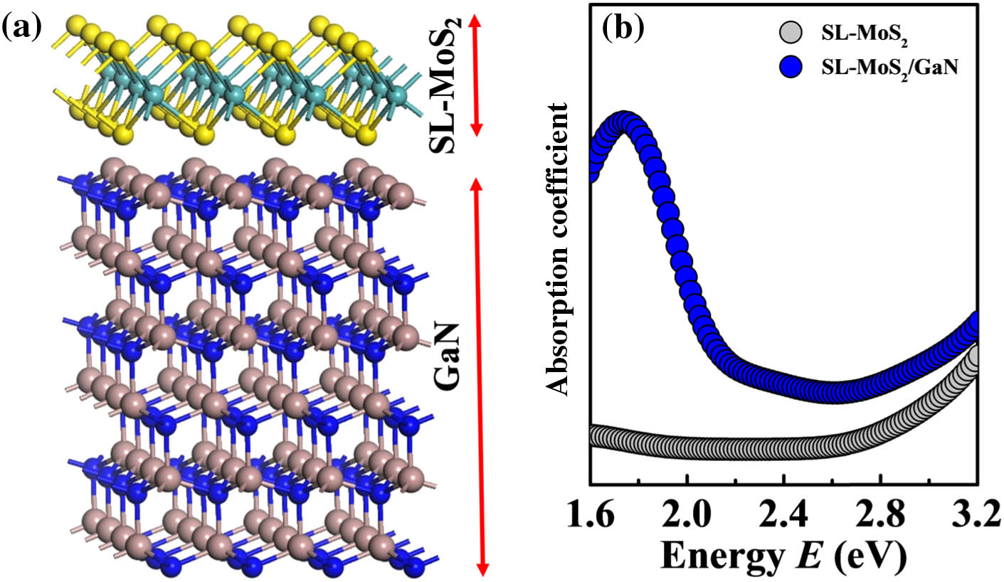
With the increasing demand for high integration and multi-color photodetection for both military and civilian applications, the research of multi-wavelength detectors has become a new research hotspot. However, current research has been mainly in visible dual- or multi-wavelength detectors, while integration of both visible light and ultraviolet (UV) dual-wavelength detectors has rarely been studied. In this work, large-scale and high-quality monolayer MoS2 was grown by the chemical vapor deposition method on transparent free-standing GaN substrate. Monolithic integration of MoS2-based visible detectors and GaN-based UV detectors was demonstrated using common semiconductor fabrication technologies such as photolithography, argon plasma etching, and metal deposition. High performance of a 280 nm and 405 nm dual-wavelength photodetector was realized. The responsivity of the UV detector reached 172.12 A/W, while that of the visible detector reached 17.5 A/W. Meanwhile, both photodetectors achieved high photocurrent gain, high external quantum efficiency, high normalized detection rate, and low noise equivalent power. Our study extends the future application of dual-wavelength detectors for image sensing and optical communication.
Photonics Research
2019, 7(10): 10001127
Author Affiliations
Abstract
1 GPPMM Group, Xlim Research Institute, CNRS UMR 7252, University of Limoges, France
2 GLOphotonics S.A.S, 123 avenue Albert Thomas, 87060 Limoges, France
3 Department of Engineering “Enzo Ferrari”, University of Modena and Reggio Emilia, I-41125 Modena, Italy
4 Max Born Institute, Max-Born-Str. 2a, D-12489 Berlin, Germany
5 e-mail: f.benabid@xlim.fr
Historically, nonlinear optical phenomena such as spectral broadening by harmonic generation have been associated with crystals owing to their strong nonlinear refractive indices, which are in the range of 10 14 cm2/W. This association was also the result of the limited optical power available from early lasers and the limited interaction length that the laser–crystal interaction architecture could offer. Consequently, these limitations disqualified a large number of materials whose nonlinear coefficient is lower than n210 16 cm2/W as suitable materials for nonlinear optics applications. For example, it is a common practice in most of optical laboratories to consider ambient or atmospheric air as a “nonlinear optically” inert medium due to its very low nonlinear coefficient (10.10 19 cm2/W) and low density. Today, the wide spread of high-power ultra-short pulse lasers on one hand, and low transmission loss and high-power handling of Kagome hollow-core photonic crystal fiber on the other hand, provide the necessary ingredients to excite strong nonlinear optical effects in practically any gas media, regardless of how low its optical nonlinear response is. By using a single table-top 1 mJ ultra-short pulse laser and an air exposed inhibited-coupling guiding hollow-core photonic crystal fiber, we observed generation of supercontinuum and third harmonic generation when the laser pulse duration was set at 600 fs and Raman comb generation when the duration was 300 ps. The supercontinuum spectrum spans over 1000 THz and exhibits a typical spectral-density energy of 150 nJ/nm. The dispersion profile of inhibited-coupling hollow-core fiber imprints a distinctive sequence in the supercontinuum generation, which is triggered by the generation of a cascade of four-wave mixing lines and concluded by solitonic dynamics. The Raman comb spans over 300 THz and exhibits multiple sidebands originating from N2 vibrational and ro-vibrational Raman transitions. With the growing use of hollow-core photonic crystal fiber in different fields, the results can be applied to mitigate air nonlinear response when it is not desired or to use ambient air as a convenient nonlinear medium.
Photonics Research
2019, 7(10): 10001134
Author Affiliations
Abstract
Hunan Key Laboratory of Super Microstructure and Ultrafast Process, School of Physics and Electronics, Central South University, Changsha 410083, China
Here we study theoretically the optical responses of hybrid structures composed of dielectric nanostructures and quantum emitters with magnetic dipole transitions. Coherent couplings between magnetic dipole transitions and magnetic modes can occur, leading to giant modifications of the extinction spectra of the constituents in the hybrid structures. For a given hybrid structure, the extinction-cross-section spectra show linear or nonlinear behaviors depending on the strength of the excitation field. For a weak excitation, the extinction of the quantum emitters is greatly enhanced. The hybrid structure shows a dip on its extinction spectrum. For a strong excitation, the resonant extinction of the quantum emitters is weakly enhanced while the extinction spectrum is broadened obviously. The hybrid structure shows a Fano-like line shape on its extinction spectrum, which is different from that with a weak excitation. This difference is highly related to the behaviors of the magnetic polarizabilities of the quantum emitters in the hybrid structure. The optical responses of hybrid structures can be largely tuned by varying the geometric and material parameters.
Photonics Research
2019, 7(10): 10001142
Sen Gong 1,2Min Hu 1,2,*Zhenhua Wu 1,2,5Hang Pan 3[ ... ]Shenggang Liu 1,2
Author Affiliations
Abstract
1 Terahertz Research Center, School of Electronic Science and Engineering, University of Electronic Science and Technology of China, Chengdu 610054, China
2 Key Laboratory of Terahertz Technology, Ministry of Education, Chengdu 610054, China
3 Glasgow College, University of Electronic Science and Technology of China, Chengdu 610054, China
4 School of Physics and Institute for Superconducting and Electronic Materials, University of Wollongong, New South Wales 2522, Australia
5 e-mail: wuzhenhua@uestc.edu.cn
Transition radiation (TR) induced by electron–matter interaction usually demands vast accelerating voltages, and the radiation angle cannot be controlled. Here we present a mechanism of direction controllable inverse transition radiation (DCITR) in a graphene-dielectric stack excited by low-velocity electrons. The revealed mechanism shows that the induced hyperbolic-like spatial dispersion and the superposition of the individual bulk graphene plasmons (GPs) modes make the fields, which are supposed to be confined on the surface, radiate in the stack along a special radiation angle normal to the Poynting vector. By adjusting the chemical potential of the graphene sheets, the radiation angle can be controlled. And owing to the excitation of bulk GPs, only hundreds of volts for the accelerating voltage are required and the field intensity is dramatically enhanced compared with that of the normal TR. Furthermore, the presented mechanism can also be applied to the hyperbolic stack based on semiconductors in the infrared region as well as noble metals in the visible and ultraviolet region. Accordingly, the presented mechanism of DCITR is of great significance in particle detection, radiation emission, and so on.
Photonics Research
2019, 7(10): 10001154
Zhao Shi 1†He Ding 2†Hao Hong 3Dali Cheng 1[ ... ]Xing Sheng 1,*
Author Affiliations
Abstract
1 Department of Electronic Engineering and Beijing National Research Center for Information Science and Technology, Tsinghua University, Beijing 100084, China
2 Beijing Engineering Research Center of Mixed Reality and Advanced Display, School of Optics and Photonics, Beijing Institute of Technology, Beijing 100081, China
3 State Key Laboratory for Mesoscopic Physics, Collaborative Innovation Center of Quantum Matter, and School of Physics, Peking University, Beijing 100871, China
Photon upconversion with transformation of low-energy photons to high-energy photons has been widely studied and especially applied in biomedicine for sensing, stimulation, and imaging. Conventional upconversion materials rely on nonlinear luminescence processes, suffering from long decay lifetime or high excitation power. Here, we present a microscale, optoelectronic infrared-to-visible upconversion device design that can be excited at low power (1100 mW/cm2). By manipulating device geometry, illumination position, and temperature, the device luminescence decay lifetime can be tuned from tens to hundreds of nanoseconds. Based on carrier transportation and circuit dynamics, theoretical models are established to understand the transient behaviors. Compared with other mechanisms, the optoelectronic upconversion approach demonstrates the shortest luminescence lifetime with the lowest required excitation power, owing to its unique photon–electron conversion process. These features are expected to empower the device with essential capabilities for versatile applications as high-performance light emitters.
Photonics Research
2019, 7(10): 10001161
Author Affiliations
Abstract
1 National Laboratory for Physical Sciences at Microscale and Department of Modern Physics, University of Science and Technology of China, Shanghai 201315, China
2 QuantumCTek Corporation Limited, Hefei 230088, China
3 Shanghai Branch, CAS Center for Excellence and Synergetic Innovation Center in Quantum Information and Quantum Physics, University of Science and Technology of China, Shanghai 201315, China
4 Department of Materials, University of Oxford, Oxford OX1 3PH, UK
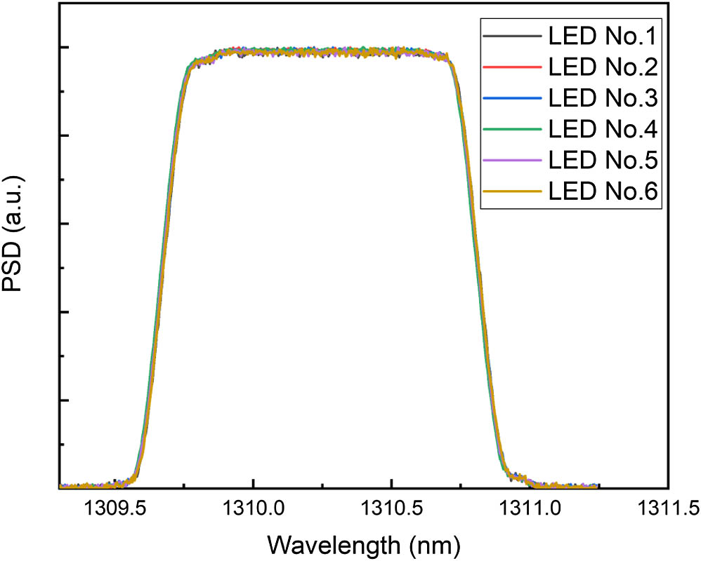
We report a quantum key distribution (QKD) system that uses light-emitting-diodes (LEDs) at 1310 nm as optical sources. Compared to the normally used laser diodes (LDs), LEDs are easier to manufacture and integrate, and thus have the potential to reduce the costs of practical systems. To demonstrate the feasibility of a low-cost, integratable QKD system that aims at meeting the demand of the last-mile secure communication, we utilize LEDs at 1310 nm as the optical sources, while using only passive optical components and only one single photon detector at the receiver’s side. With a repetition rate of 10 MHz, we obtain secure key rates of 10.9 kbps within the experimental time of 1000 s over a fiber length of 1 km.
Photonics Research
2019, 7(10): 10001169
Author Affiliations
Abstract
1 Department of Electrical, Computer & Energy Engineering, University of Colorado Boulder, Boulder, Colorado 80309, USA
2 e-mail: Mingming.Nie@colorado.edu
3 e-mail: ShuWei.Huang@colorado.edu
We present the first design and analysis of a solid-state Mamyshev oscillator. We utilize the phase-mismatched cascaded quadratic nonlinear process in a periodically poled lithium niobate waveguide to generate substantial spectral broadening for Mamyshev mode locking. The extensive spectral broadening bridges the two narrowband gain media in the two arms of the same cavity, leading to a broadband mode locking not attainable with either gain medium alone. Two pulses are coupled out of the cavity, and each of the output pulses carries a pulse energy of 25.3 nJ at a repetition rate of 100 MHz. The 10 dB bandwidth of 2.1 THz supports a transform-limited pulse duration of 322 fs, more than 5 times shorter than what can be achieved with either gain medium alone. Finally, effects of group velocity mismatch, group velocity dispersion, and nonlinear saturation on the performance of Mamyshev mode locking are numerically discussed in detail.
Photonics Research
2019, 7(10): 10001175
Author Affiliations
Abstract
1 Center for Advanced Material Diagnostic Technology, College of Engineering Physics, Shenzhen Technology University, Shenzhen 518118, China
2 Shenzhen Key Laboratory of Laser Engineering, Shenzhen University, Shenzhen 518060, China
3 College of New Materials and New Energies, Shenzhen Technology University, Shenzhen 518118, China
4 Institute of Applied Physics & Materials Engineering, Faculty of Science and Technology, University of Macau, Macau, China
Carbon nanodots (C-dots) with a uniform size of about 2 nm are synthesized via in situ pyrolysis of n-propylamine that is confined in the nanochannels of zeolite Linde Type A (LTA). The as-synthesized C-dots@LTA composite shows nonlinear optical saturable absorption properties in a broad wavelength band and can be used as saturable absorber (SA) to generate ultrafast pulsed fiber lasers. By inserting a zeolite LTA single crystal hosting C-dots into the fiber laser cavity, mode-locked fiber lasers with long-term operation stability at 1.5 μm and 1 μm are achieved. These results show that the C-dots@LTA are a promising SA material for ultrafast pulsed fiber laser generation in a broad wavelength band. To the best of our knowledge, this is the first demonstration of a C-dots@LTA-based mode-locked fiber laser.
Photonics Research
2019, 7(10): 10001182
Author Affiliations
Abstract
1 Research Laboratory of Electronics, Massachusetts Institute of Technology, Cambridge, Massachusetts 02139, USA
2 Technion—Israel Institute of Technology, Faculty of Mechanical Engineering, Haifa 3200003, Israel
We fabricate a tapered fiber coupler, position it near an ultrahigh-Q resonator made from a microdroplet, and experimentally measure stimulated Raman emission. We then calculate the molecular vibrational mode associated with each of the Raman lines and present it in a movie. Our Raman laser lines show themselves at a threshold of 160 μW input power, the cold-cavity quality factor is 250 million, and mode volume is 23 μm3. Both pump and Raman laser modes overlap with the liquid phase instead of just residually extending to the fluid.
Photonics Research
2019, 7(10): 10001188
Author Affiliations
Abstract
1 Department of Electrical and Computer Engineering, Texas A&M University, College Station, Texas 77843, USA
2 Department of Materials Science and Engineering, Texas A&M University, College Station, Texas 77843, USA
3 Center for Remote Health Technologies and Systems, Texas A&M University, College Station, Texas 77843, USA
4 The Center for Functional Nanomaterials, Brookhaven National Laboratory, Upton, New York 11973, USA
The mid-infrared (mid-IR) second-order optical nonlinearity of the barium titanate (BTO) thin films was characterized by second harmonic generation (SHG). The epitaxial BTO thin films were grown on strontium titanate substrates by pulsed-laser deposition. From the azimuthal-dependent polarized SHG measurements, the tensorial optical nonlinear coefficients, dij, and ferroelectric domain fraction ratio, δAY/δAz, were resolved. Strong SHG signals were obtained at the pumping laser wavelength λ between 3.0 and 3.6 μm. The SHG intensity was linearly dependent upon the square of the pumping laser power. The broadband mid-IR optical nonlinearity enables BTO thin films for applications in chip-scale quantum optics and nonlinear integrated photonic circuits.
Photonics Research
2019, 7(10): 10001193
Yuhua Li 1†Kun Zhu 2†Zhe Kang 2,5,*Wai Lok Ho 1[ ... ]Sai Tak Chu 1,6,*
Author Affiliations
Abstract
1 Department of Physics, City University of Hong Kong, Hong Kong, China
2 Photonics Research Centre, Department of Electronic and Information Engineering, The Hong Kong Polytechnic University, Hong Kong, China
3 QXP Technology Inc., Xi’an 710119, China
4 State Key Laboratory of Transient Optics and Photonics, XIOPM, CAS, Xi’an 710119, China
5 e-mail: zhe.kang@polyu.edu.hk
6 e-mail: saitchu@cityu.edu.hk
Passive all-optical signal processors that overcome the electronic bottleneck can potentially be the enabling components for the next-generation high-speed and lower power consumption systems. Here, we propose and experimentally demonstrate a CMOS-compatible waveguide and its application to the all-optical analog-to-digital converter (ADC) under the nonlinear spectral splitting and filtering scheme. As the key component of the proposed ADC, a 50 cm long high-index doped silica glass spiral waveguide is composed of a thin silicon-nanocrystal (Si-nc) layer embedded in the core center for enhanced nonlinearity. The device simultaneously possesses low loss (0.16 dB/cm at 1550 nm), large nonlinearity (305 W 1/km at 1550 nm), and negligible nonlinear absorption. A 2-bit ADC basic unit is achieved when pumped by the proposed waveguide structure at the telecom band and without any additional amplification. Simulation results that are consistent with the experimental ones are also demonstrated, which further confirm the feasibility of the proposed scheme for larger quantization resolution. This demonstrated approach enables a fully monolithic solution for all-optical ADC in the future, which can digitize broadband optical signals directly at low power consumption. This has great potential on the applications of high-speed optical communications, networks, and signal processing systems.
Photonics Research
2019, 7(10): 10001200