Photonics Research
Search

2019, 7(2) Column

MORE

Photonics Research 第7卷 第2期

Author Affiliations
Abstract
1 State Key Laboratory of Electronic Thin Films and Integrated Devices, School of Optoelectronic Science and Engineering, University of Electronic Science and Technology of China, Chengdu 610054, China
2 School of Optical and Electronic Information, Huazhong University of Science and Technology, Wuhan 430074, China
3 Aston Institute of Photonic Technologies (AiPT), Aston University, Birmingham B4 7ET, UK
4 e-mail: yanzhijin@gmail.com
5 e-mail: l.zhang@aston.ac.uk
We demonstrate a stable conventional soliton in a Tm-doped hybrid mode-locked fiber laser by employing a homemade all-fiber Lyot filter (AFLF) and a single-wall carbon nanotube. The AFLF, designed by sandwiching a piece of polarization-maintained fiber (PMF) with two 45° tilted fiber gratings inscribed by a UV laser in PMF with a phase-mask scanning technique, shows large filter depth of 9 dB and small insertion loss of 0.8 dB. By optimizing the free spectral range of the AFLF, the Kelly sidebands of a conventional soliton centered at 1966.4 nm can be dramatically suppressed without impairing the main shape of the soliton spectrum. It gives the pulse duration of 1.18 ps and bandwidth of 3.8 nm. By adjusting the temperature of the PMF of the AFLF from 7°C to 60°C, wavelength tunable soliton pulses ranging from 1971.62 nm to 1952.63 nm are also obtained. The generated soliton pulses can be precisely tuned between 1971.62 nm and 1952.63 nm by controlling the temperature of the AFLF.
Photonics Research
2019, 7(2): 02000103
Lu Xu 1Jie Hou 1Haitao Tang 1Yuan Yu 1,2,3,*[ ... ]Xinliang Zhang 1,2
Author Affiliations
Abstract
1 Wuhan National Laboratory for Optoelectronics, Huazhong University of Science and Technology, Wuhan 430074, China
2 School of Optical and Electrical Information, Huazhong University of Science and Technology, Wuhan 430074, China
3 e-mail: yuan_yu@hust.edu.cn
4 e-mail: yuyu@mail.hust.edu.cn
We demonstrate a silicon-based microwave photonic filter (MPF) with flattop passband and adjustable bandwidth. The proposed MPF is realized by using a 10th-order microring resonator (MRR) and a photodetector, both of which are integrated on a photonic chip. The full width at half-maximum (FWHM) bandwidth of the optical filter achieved at the drop port of the 10th-order MRR is 21.6 GHz. The ripple of the passband is less than 0.3 dB, while the rejection ratio is 32 dB. By adjusting the deviation of the optical carrier wavelength from the center wavelength of the optical bandpass filter, the bandwidth of the MPF can be greatly changed. In the experiment, the FWHM bandwidth of the proposed MPF is tuned from 5.3 to 19.5 GHz, and the rejection ratio is higher than 30 dB.
Photonics Research
2019, 7(2): 02000110
Bo Fu 1,2Jin Li 3,4Zhang Cao 1,2Daniel Popa 3,*
Author Affiliations
Abstract
1 Beijing Advanced Innovation Center for Big Data-Based Precision Medicine, Interdisciplinary Innovation Institute of Medicine and Engineering, Beihang University, Beijing 100191, China
2 School of Instrumentation and Optoelectronic Engineering, Beihang University, Beijing 100191, China
3 Department of Engineering, University of Cambridge, Cambridge CB3 0FA, UK
4 e-mail: jl918@cam.ac.uk
We report bound states of solitons from a harmonic mode-locked fiber laser based on a solution-processed graphene saturable absorber. Stable soliton pairs, 26.2 ps apart, are generated with 720 fs duration. By simply increasing the pump power, the laser can also generate harmonic mode-locking with harmonics up to the 26th order (409.6 MHz repetition rate). This is a simple, low-cost, all-fiber, versatile multifunction ultrafast laser that could be used for many applications.
Photonics Research
2019, 7(2): 02000116
Author Affiliations
Abstract
1 Laboratory of Solid-State Optoelectronics Information Technology, Institute of Semiconductors, Chinese Academy of Sciences, Beijing 100083, China
2 State Key Laboratory on Integrated Optoelectronics, Institute of Semiconductors, Chinese Academy of Sciences, Beijing 100083, China
3 Center of Materials Science and Optoelectronics Engineering, University of Chinese Academy of Sciences, Beijing 100049, China
4 Institute of Solid State Physics and Center of Nanophotonics, Technische Universität Berlin, Hardenbergstrasse 36, 10623 Berlin, Germany
5 Bimberg Chinese-German Center for Green Photonics of the Chinese Academy of Sciences at CIOMP, Changchun 130033, China
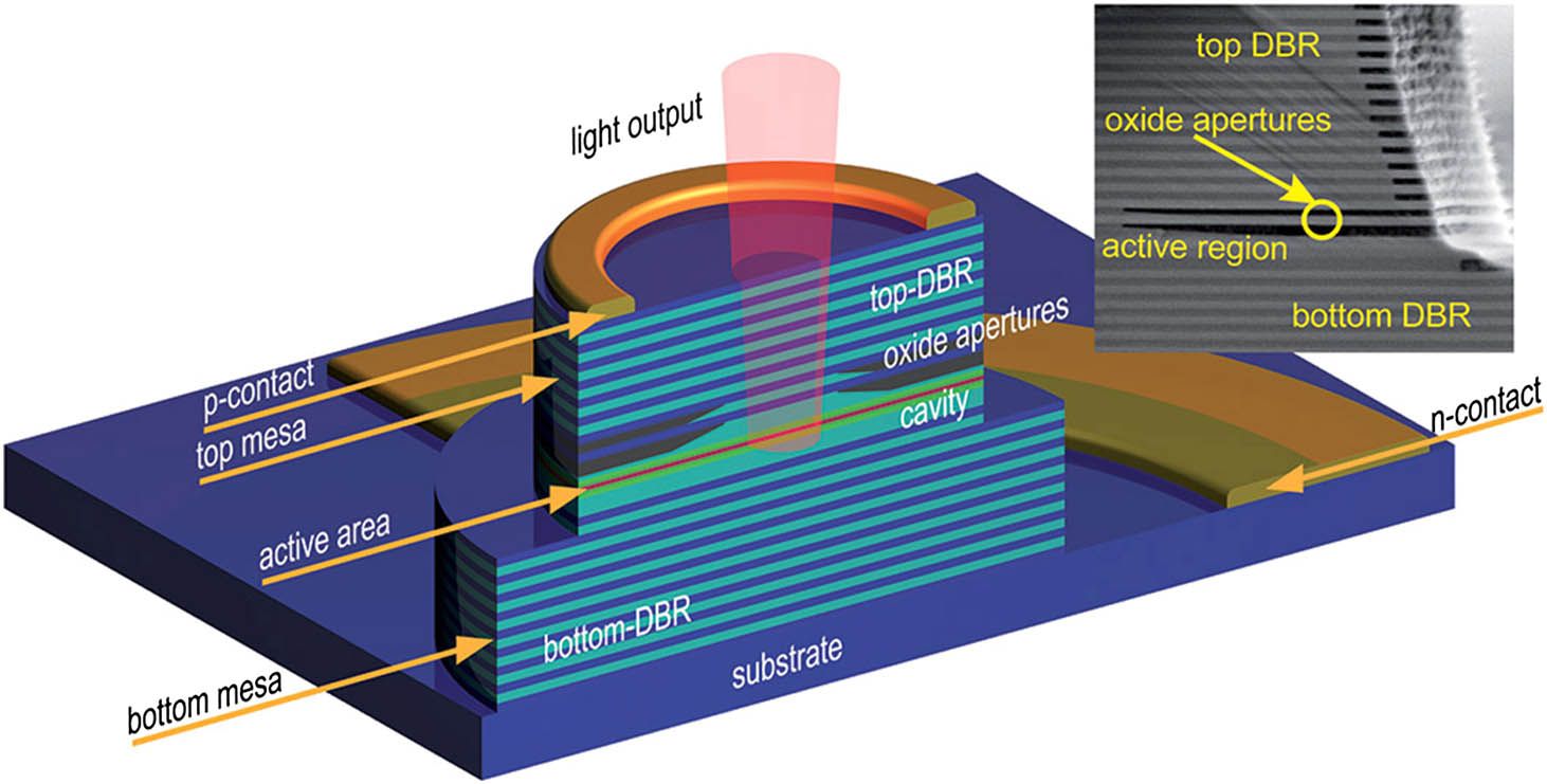
Vertical-cavity surface-emitting lasers (VCSELs) are the ideal optical sources for data communication and sensing. In data communication, large data rates combined with excellent energy efficiency and temperature stability have been achieved based on advanced device design and modulation formats. VCSELs are also promising sources for photonic integrated circuits due to their small footprint and low power consumption. Also, VCSELs are commonly used for a wide variety of applications in the consumer electronics market. These applications range from laser mice to three-dimensional (3D) sensing and imaging, including various 3D movement detections, such as gesture recognition or face recognition. Novel VCSEL types will include metastructures, exhibiting additional unique properties, of largest importance for next-generation data communication, sensing, and photonic integrated circuits.
Photonics Research
2019, 7(2): 02000121
Hongbo Lu 1,2,7,*Cheng Wei 1Qiang Zhang 1Miao Xu 1,2[ ... ]Longzhen Qiu 1,2
Author Affiliations
Abstract
1 Key Laboratory of Special Display Technology, National Engineering Laboratory of Special Display Technology, State Key Laboratory of Advanced Display Technology, Academy of Opto-Electronic Technology, Hefei University of Technology, Hefei 230009, China
2 Key Laboratory of Advanced Functional Materials and Devices, Anhui Province, School of Chemistry and Chemical Engineering, Hefei University of Technology, Hefei 230009, China
3 School of Instrument Science and Opto-Electronics Engineering, Hefei University of Technology, Hefei 230009, China
4 Aston Institute of Photonic Technologies, Aston University, Birmingham B4 7ET, UK
5 State Key Laboratory of Environment-Friendly Energy Materials, Southwest University of Science and Technology, Mianyang 621000, China
6 e-mail: zhijiahu@hfut.edu.cn
7 e-mail: bozhilu@hfut.edu.cn
Electrically responsive photonic crystals represent one of the most promising intelligent material candidates for technological applications in optoelectronics. In this research, dye-doped polymer-stabilized cholesteric liquid crystals (PSCLCs) with negative dielectric anisotropy were fabricated, and mirrorless lasing with an electrically tunable wavelength was successfully achieved. Unlike conventional liquid-crystal lasers, the proposed laser aided in tuning the emission wavelength through controlling the reflection bandwidth based on gradient pitch distribution. The principal advantage of the electrically controlled dye-doped PSCLC laser is that the electric field is applied parallel to the helical axis, which changes the pitch gradient instead of rotating the helix axis, thus keeping the heliconical structure intact during lasing. The broad tuning range (110 nm) of PSCLC lasers, coupled with their stable emission performance, continuous tunability, and easy fabrication, leads to its numerous potential applications in intelligent optoelectronic devices, such as sensing, medicine, and display.
Photonics Research
2019, 7(2): 02000137
Author Affiliations
Abstract
1 National Institute of LED on Silicon Substrate, Nanchang University, Nanchang 330096, China
2 Nanchang Yellow Green Lighting Company Limited, Nanchang 330096, China
3 e-mail: liujunlin@ncu.edu.cn
Realization of efficient yellow-light-emitting diodes (LEDs) has always been a challenge in solid-state lighting. Great effort has been made, but only slight advancements have occurred in the past few decades. After comprehensive work on InGaN-based yellow LEDs on Si substrate, we successfully made a breakthrough and pushed the wall-plug efficiency of 565-nm-yellow LEDs to 24.3% at 20 A/cm2 and 33.7% at 3 A/cm2. The success of yellow LEDs can be credited to the improved material quality and reduced compressive strain of InGaN quantum wells by a prestrained layer and substrate, as well as enhanced hole injection by a 3D pn junction with V-pits.
Photonics Research
2019, 7(2): 02000144
Author Affiliations
Abstract
1 Key Laboratory of Opto-Electronic Information Technology (Tianjin University), Ministry of Education, School of Precision Instruments and Opto-Electronics Engineering, Tianjin University, Tianjin 300072, China
2 Tianjin Key Laboratory of Low Dimensional Materials Physics and Preparing Technology, School of Science, Tianjin University, Tianjin 300072, China
3 Center of Material Science, National University of Defense Technology, Changsha 410073, China
Because they possess excellent visible light absorption properties, lead-free colloidal copper-based chalcogenide quantum dots (QDs) have emerged in photoelectronic fields. By means of localized surface plasmonic resonance (LSPR), the absorption properties of QDs can be enhanced. In this paper, we fabricate a lead-free CuInSe2 QD field effect phototransistor (FEpT) by utilizing the LSPR enhancement of Au nanoparticles (NPs). The plasmonic FEpT demonstrates responsivity up to 2.7 μA·W 1 and a specific detectivity of 7×10³ Jones at zero bias under illumination by a 532 nm laser, values that are enhanced by approximately 200% more than devices without Au NPs. Particularly, the FEpT exhibits a multi-wavelength response, which is photoresponsive to 405, 532, and 808 nm irradiations, and presents stability and reproducibility in the progress of ON–OFF cycles. Furthermore, the enhancement induced by Au NP LSPR can be interpreted by finite-difference time domain simulations. The low-cost solution-based process and excellent device performance strongly underscore lead-free CuInSe2 QDs as a promising material for self-powered photoelectronic applications, which can be further enhanced by Au NP LSPR.
Photonics Research
2019, 7(2): 02000149
Author Affiliations
Abstract
1 Department of Electrical Engineering, Columbia University, New York, New York 10027, USA
2 Tyndall National Institute, University College Cork, Cork, Ireland
We report on the first monolithically integrated microring-based optical switch in the switch-and-select architecture. The switch fabric delivers strictly non-blocking connectivity while completely canceling the first-order crosstalk. The 4×4 switching circuit consists of eight silicon microring-based spatial (de-)multiplexers interconnected by a Si/SiN dual-layer crossing-free central shuffle. Analysis of the on-state and off-state power transfer functions reveals the extinction ratios of individual ring resonators exceeding 25 dB, leading to switch crosstalk suppression of up to over 50 dB in the switch-and-select topology. Optical paths are assessed, showing losses as low as 0.1 dB per off-resonance ring and 0.5 dB per on-resonance ring. Photonic switching is actuated with integrated micro-heaters to give an 24 GHz passband. The fully packaged device is flip-chip bonded onto a printed circuit board breakout board with a UV-curved fiber array.
Photonics Research
2019, 7(2): 02000155
Author Affiliations
Abstract
1 Department of Electronic Engineering, Xiamen University, Xiamen 361005, China
2 Jiangsu Key Laboratory of Advanced Laser Materials and Devices, School of Physics and Electronic Engineering, Jiangsu Normal University, Xuzhou 221116, China
3 School of Physics Science and Engineering, Institute for Advanced Study, Tongji University, Shanghai 200092, China
4 Department of Physics, Sofia University, 5 James Bourchier Blvd., 1164 Sofia, Bulgaria
5 e-mail: xdxu79@jsnu.edu.cn
We report on a diode-end-pumped high-power and high-energy Nd:YAG single-crystal fiber laser at 1834 nm. Two 808 nm diodes injecting about 58 W pump power into the Nd:YAG fiber have generated 3.28 W continuous-wave and 1.66 W Cr:ZnSe-based passively Q-switched lasers. Slope efficiencies with respect to pump powers are 8.7% for the continuous-wave laser and 4.9% for the Q-switched laser. The extracted maximum pulse energy is about 266.9 μJ, and the corresponding maximum pulse peak power is 2.54 kW. These performances greatly surpass previous results regarding this specific laser emission because the laser gain medium in the form of fiber can significantly mitigate thermally induced power saturation thanks to its significantly reduced thermal lensing effect. Single-crystal fiber lasers show great potential for high average power, pulse energy, and peak power.
Photonics Research
2019, 7(2): 02000162
Meng Wang 1,2,3Zefeng Wang 1,2,3,*Le Liu 1,2,3Qihao Hu 1,2,3[ ... ]Xiaojun Xu 1,2,3
Author Affiliations
Abstract
1 College of Advanced Interdisciplinary Studies, National University of Defense Technology, Changsha 410073, China
2 State Key Laboratory of Pulsed Power Laser Technology, Changsha 410073, China
3 Hunan Provincial Key Laboratory of High Energy Laser Technology, Changsha 410073, China
The average power of fiber lasers has been scaled deeply into the kW regime in the past years. However, stimulated Raman scattering (SRS) is still a major factor limiting further power scaling. Here, we have demonstrated for the first time, to the best of our knowledge, the suppression of SRS in a half 10 kW tandem pumping fiber amplifier using chirped and tilted fiber Bragg gratings (CTFBGs). With specially self-designed and manufactured CTFBGs inserted between the seed laser and the amplifier stage, a maximum SRS suppression ratio of >15 dB in spectrum is observed with no reduction in laser efficiency. With one CTFBG, the effective output power is improved to 3.9 kW with a beam quality M2 factor of 1.7 from <3.5 kW with an M2 factor of >2; with two CTFBGs, the effective laser power reaches 4.2 kW with an increasing ratio of 20% and an M2 factor of 1.8, and further power improvement is limited by the power and performance of the 1018 nm pump sources. This work provides an effective SRS suppression method for high-power all-fiber lasers, which is useful for further power scaling of these systems.
Photonics Research
2019, 7(2): 02000167
Author Affiliations
Abstract
1 Wuhan National Laboratory for Optoelectronics, School of Optical and Electronic Information, Huazhong University of Science and Technology, Wuhan 430074, China
2 State Key Laboratory of Optical Communication Technologies and Networks, Wuhan Research Institute of Posts and Telecommunications, Wuhan 430074, China
3 e-mail: xxiao@wri.com.cn
Photonic-assisted microwave frequency identification with distinct features, including wide frequency coverage and fast tunability, has been conceived as a key technique for applications such as cognitive radio and dynamic spectrum access. The implementations based on compact integrated photonic chips have exhibited distinct advantages in footprint miniaturization, light weight, and low power consumption, in stark contrast with discrete optical-fiber-based realization. However, reported chip-based instantaneous frequency measurements can only operate at a single-tone input, which stringently limits their practical applications that require wideband identification capability in modern RF and microwave applications. In this article, we demonstrate, for the first time, a wideband, adaptive microwave frequency identification solution based on a silicon photonic integrated chip, enabling the identification of different types of microwave signals from 1 to 30 GHz, including single-frequency, multiple-frequency, chirped-frequency, and frequency-hopping microwave signals, and even their combinations. The key component is a high Q-factor scanning filter based on a silicon microring resonator, which is used to implement frequency-to-time mapping. This demonstration opens the door to a monolithic silicon platform that makes possible a wideband, adaptive, and high-speed signal identification subsystem with a high resolution and a low size, weight, and power (SWaP) for mobile and avionic applications.
Photonics Research
2019, 7(2): 02000172
Author Affiliations
Abstract
1 Laser & Fiber Electronics Group, Faculty of Electronics, Wroclaw University of Science and Technology, Wybrzeze Wyspianskiego 27, 50-370 Wroclaw, Poland
2 Department of Optics and Photonics, Faculty of Fundamental Problems of Technology, Wroclaw University of Science and Technology, Wybrzeze Wyspianskiego 27, 50-370 Wroclaw, Poland
3 Laboratory of Optical Fiber Technology, Maria Curie-Sklodowska University, pl. M. Curie-Sklodowskiej 3, Lublin, Poland
We present an ultrabroadband, high-speed wavelength-swept source based on a self-modulated femtosecond oscillator. Photonic crystal fiber was pumped by a mode-locked Yb:CaF2 laser, resulting in a strong spectral broadening from 485 to 1800 nm. The pump laser cavity could be realigned in order to achieve total mode-locking of the longitudinal and transverse TEM00 and TEM01 electromagnetic modes. This led to spatial oscillations of the output beam, which induced modulation of the coupling efficiency to the fiber. Due to the fact that nonlinear spectral broadening was intensity dependent, this mechanism introduced wavelength sweeping at the fiber output. The sweeping rate could be adjusted between 7 and 21.5 MHz by changing the geometry of the pump cavity. By controlling the ratio of the transverse mode amplitudes, we were able to tune the sweeping bandwidth, eventually covering both the 1300 nm and 1700 nm bioimaging transparency windows. When compared with previously demonstrated wavelength-swept sources, our concept offers much broader tunability and higher speed. Moreover, it does not require an additional intensity modulator.
Photonics Research
2019, 7(2): 02000182
Guangwei Chen 1,2Wenlei Li 1,2Guomei Wang 1,2Wenfu Zhang 1,2[ ... ]Wei Zhao 1,2,4,*
Author Affiliations
Abstract
1 State Key Laboratory of Transient Optics and Photonics, Xi’an Institute of Optics and Precision Mechanics, Chinese Academy of Sciences, Xi’an 710119, China
2 University of Chinese Academy of Sciences (UCAS), Beijing 100049, China
3 e-mail: zengchao@opt.cn
4 e-mail: weiz@opt.ac.cn
We demonstrate a passively mode-locked all-fiber laser incorporating a piece of graded-index multimode fiber as a mode-locking modulator based on a nonlinear multimodal interference technique, which generates two types of coexisting high-energy ultrashort pulses [i.e., the conventional soliton (CS) and the stretched pulse (SP)]. The CS with pulse energy as high as 0.38 nJ is obtained at the pump level of 130 mW. When the pump increases to 175 mW, the high-energy SP occurs at a suitable nonlinear phase bias and its pulse energy can reach 4 nJ at a 610 mW pump. The pulse durations of the generated CS and SP are 2.3 ps and 387 fs, respectively. The theory of nonlinear fiber optics, single-shot spectral measurement by the dispersive Fourier-transform technique, and simulation methods based on the Ginzburg–Landau equation are provided to characterize the laser physics and reveal the underlying principles of the generated CS and SP. A rogue wave, observed between the CS and SP regions, mirrors the laser physics behind the dynamics of generating a high-energy SP from a CS. The proposed all-fiber laser is versatile, cost-effective and easy to integrate, which provides a promising solution for high-energy pulse generation.
Photonics Research
2019, 7(2): 02000187
Author Affiliations
Abstract
1 School of Electronics and Computer Science, University of Southampton, SO17 1BJ, UK
2 Optoelectronics Research Centre, University of Southampton, SO17 1BJ, UK
3 School of Electrical and Electronic Engineering, Nanyang Technological University, Singapore, Singapore
We demonstrate low-loss hydrogenated amorphous silicon (a-Si:H) waveguides by hot-wire chemical vapor deposition (HWCVD). The effect of hydrogenation in a-Si at different deposition temperatures has been investigated and analyzed by Raman spectroscopy. We obtained an optical quality a-Si:H waveguide deposited at 230°C that has a strong Raman peak shift at 480 cm 1, peak width (full width at half-maximum) of 68.9 cm 1, and bond angle deviation of 8.98°. Optical transmission measurement shows a low propagation loss of 0.8 dB/cm at the 1550 nm wavelength, which is the first, to our knowledge, report for a HWCVD a-Si:H waveguide.
Photonics Research
2019, 7(2): 02000193
Author Affiliations
Abstract
1 Electrical, Computer and Biomedical Engineering Department, University of Pavia, Pavia 27100, Italy
2 Optoelectronics Research Centre, Highfield Campus, University of Southampton, Southampton SO17 1BJ, UK
3 Photonic Packaging Group, Tyndall National Institute, Lee Maltings Complex, Cork T12R5CP, Ireland
Over the last 20 years, silicon photonics has revolutionized the field of integrated optics, providing a novel and powerful platform to build mass-producible optical circuits. One of the most attractive aspects of silicon photonics is its ability to provide extremely small optical components, whose typical dimensions are an order of magnitude smaller than those of optical fiber devices. This dimension difference makes the design of fiber-to-chip interfaces challenging and, over the years, has stimulated considerable technical and research efforts in the field. Fiber-to-silicon photonic chip interfaces can be broadly divided into two principle categories: in-plane and out-of-plane couplers. Devices falling into the first category typically offer relatively high coupling efficiency, broad coupling bandwidth (in wavelength), and low polarization dependence but require relatively complex fabrication and assembly procedures that are not directly compatible with wafer-scale testing. Conversely, out-of-plane coupling devices offer lower efficiency, narrower bandwidth, and are usually polarization dependent. However, they are often more compatible with high-volume fabrication and packaging processes and allow for on-wafer access to any part of the optical circuit. In this paper, we review the current state-of-the-art of optical couplers for photonic integrated circuits, aiming to give to the reader a comprehensive and broad view of the field, identifying advantages and disadvantages of each solution. As fiber-to-chip couplers are inherently related to packaging technologies and the co-design of optical packages has become essential, we also review the main solutions currently used to package and assemble optical fibers with silicon-photonic integrated circuits.
Photonics Research
2019, 7(2): 02000201
Author Affiliations
Abstract
1 Key Laboratory of Advanced Micro/Nano Electronic Devices & Smart Systems and Applications, College of Information Science and Electronic Engineering, Zhejiang University, Hangzhou 310027, China
2 Zhejiang University—University of Illinois at Urbana—Champaign Institute, Zhejiang University, Haining 314400, China
Slow light, a technology to control the optical signal by reducing the group velocity, has been widely studied to obtain enhanced nonlinearities and increased phase shifts owing to its promoting of the light–matter interaction ability. In this work, a wideband slow light is achieved in a simple one-dimensional fishbone grating waveguide. A flat band indicating slow light with a group index of 13 and bandwidth over 10 nm is obtained by the plane wave expansion calculation, and the corresponding experimental results agree well with the theoretical prediction. A step taper is designed to compensate the coupling loss. The proposed fishbone grating waveguide is a good candidate for wideband slow light devices in light communication.
Photonics Research
2019, 7(2): 02000240