Photonics Research
Search

2019, 7(8) Column

MORE

Photonics Research 第7卷 第8期

Author Affiliations
Abstract
1 Department of Electrical and Computer Engineering, University of Wisconsin Madison, Madison, Wisconsin 53706, USA
2 Department of Aeronautics and Astronautics, Massachusetts Institute of Technology, Cambridge, Massachusetts 02139, USA
3 Department of Statistics, Columbia University, New York, New York 10027, USA
We show optical waves passing through a nanophotonic medium can perform artificial neural computing. Complex information is encoded in the wavefront of an input light. The medium transforms the wavefront to realize sophisticated computing tasks such as image recognition. At the output, the optical energy is concentrated in well-defined locations, which, for example, can be interpreted as the identity of the object in the image. These computing media can be as small as tens of wavelengths and offer ultra-high computing density. They exploit subwavelength scatterers to realize complex input/output mapping beyond the capabilities of traditional nanophotonic devices.
Photonics Research
2019, 7(8): 08000823
Author Affiliations
Abstract
1 Optoelectronics Research Centre, University of Southampton, Southampton SO17 1BJ, UK
2 State Key Laboratory of Advanced Optical Communication Systems and Networks, School of Electronics Engineering and Computer Science, Peking University, Beijing 100871, China
3 Silicon Technologies Centre of Excellence, Nanyang Technological University, Singapore 639798, Singapore
4 Centre de Nanosciences et de Nanotechnologies, CNRS, Univ. Paris-Sud, Université Paris-Saclay, C2N—Palaiseau, 91120 Palaiseau, France
We report mid-infrared Ge-on-Si waveguide-based PIN diode modulators operating at wavelengths of 3.8 and 8 μm. Fabricated 1-mm-long electro-absorption devices exhibit a modulation depth of >35 dB with a 7 V forward bias at 3.8 μm, and a similar 1-mm-long Mach–Zehnder modulator has a Vπ·L of 0.47 V·cm. Driven by a 2.5Vpp RF signal, 60 MHz on-off keying modulation was demonstrated. Electro-absorption modulation at 8 μm was demonstrated preliminarily, with the device performance limited by large contact separation and high contact resistance.
Photonics Research
2019, 7(8): 08000828
Author Affiliations
Abstract
1 Center for Advanced Material Diagnostic Technology, College of Engineering Physics, Shenzhen Technology University, Shenzhen 518118, China
2 Guangdong Provincial Key Laboratory of Mico/Nano Optomechatronics Engineering, College of Optoelectronic Engineering, Shenzhen University, Shenzhen 518060, China
3 College of New Materials and New Energies, Shenzhen University of Technology, Shenzhen 518118, China
Perovskite quantum dots (QDs) are of great interest due to their outstanding optoelectronic properties and tremendous application potential. Improving photoluminescence (PL) spectra in all-inorganic perovskite QDs is of great importance for performance enhancement. In this work, the PL quantum yield of the CsPbBr3 perovskite QDs is enhanced from 70% to 95% with increasing radiation pressure. Such enhancement is attributed to the increased binding energy of self-trapped excitons (STEs) upon radiation pressure, which is consistent with its blue-shifted PL and other characterization results. Furthermore, we study ultrafast absorption spectroscopy and find that the dynamics of relaxation from free excitons to STEs in radiation pressure CsPbBr3 QDs is ascribed to stronger electron–phonon coupling in the contracted octahedral structure. It is further demonstrated that radiation pressure can boost the PL efficiency and explore effectively the relationship between the structure and optical properties.
Photonics Research
2019, 7(8): 08000837
Author Affiliations
Abstract
1 School of Science, Beijing University of Posts and Telecommunications, Beijing 100876, China
2 State Key Laboratory of Information Photonics and Optical Communications, Beijing University of Posts and Telecommunications, Beijing 100876, China
We designed a low-filling-factor and polarization-sensitive superconducting nanowire single photon detector (SNSPD), which can achieve a high absorption efficiency and counting rate simultaneously. Numerical simulations show that high absorption efficiency can be achieved by low-filling-factor SNSPDs with a silicon slot and silver reflector. The absorptance of the NbN nanowire for a transverse magnetic (TM) wave at the wavelength of 1550 nm can be 84.4% when the filling factor is only 16.5%, and the corresponding polarization extinction ratio (PER) is 562.9; the absorptance of the NbN nanowire for a transverse electric (TE) wave can be 67.0% when the filling factor is only 11.7%, and the PER is 7.4.
Photonics Research
2019, 7(8): 08000847
Author Affiliations
Abstract
1 College of Optical and Electronic Technology, China Jiliang University, Hangzhou 310018, China
2 e-mail: 16a0402091@cjlu.edu.cn
3 e-mail: dnwang@cjlu.edu.cn
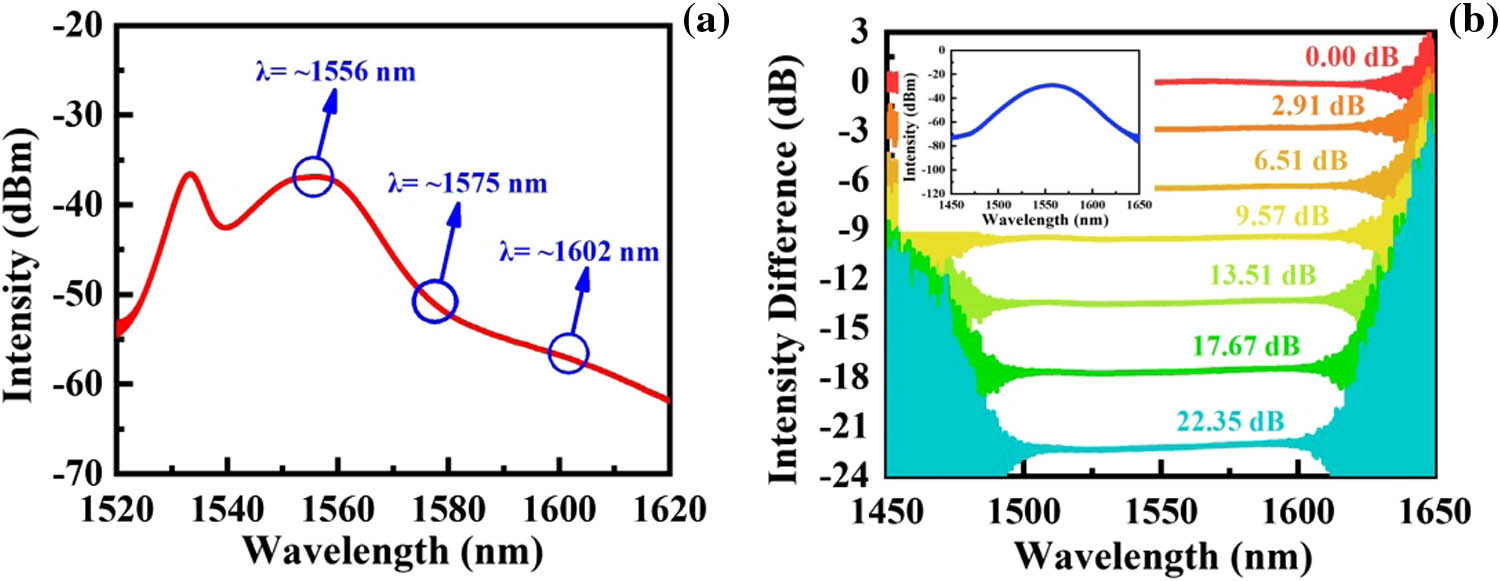
A wavelength-tunable and dual-wavelength mode-locking operation is achieved in an Er-doped fiber laser using a hybrid no-core fiber graded index multimode fiber as the saturable absorber. In the tuning operation, continuously wavelength-tunable pulses with a tuning range of 46.7 nm, stable 3-dB bandwidth of around 5 nm, and pulse duration of
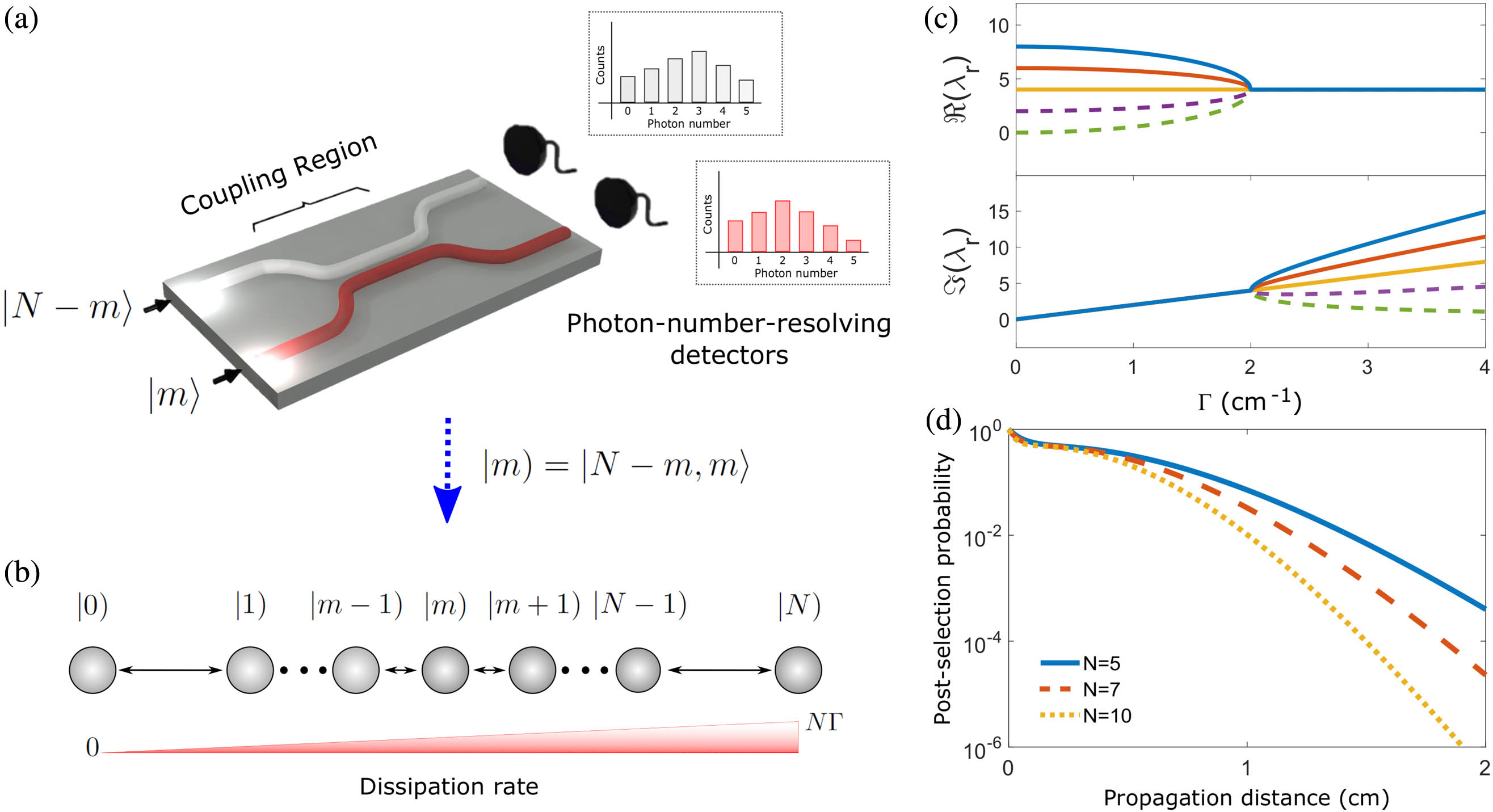
 850 fs are obtained by increasing the intracavity loss of a variable optical attenuator. In the dual-wavelength operation, the two solitons at different wavelengths demonstrate the characteristics of mutual coherence. By increasing the intracavity loss, the spectral spacing can be tuned from 11 to 33.01 nm while maintaining the coherence of the solitons. Such coherent solitons have high potential for applications in dual-comb frequency and multicolor pulses in nonlinear microscopy.
Photonics Research
2019, 7(8): 08000853
Author Affiliations
Abstract
1 Instituto de Ciencias Nucleares, Universidad Nacional Autónoma de México, Apartado Postal 70-543, 04510 Cd. Mx., Mexico
2 Max-Born-Institut, Max-Born-Straße 2A, 12489 Berlin, Germany
3 Humboldt-Universität zu Berlin, Institut für Physik, AG Theoretische Optik & Photonik, D-12489 Berlin, Germany
4 Tecnológico de Monterrey, Escuela de Ingeniería y Ciencias, Ave. Eugenio Garza Sada 2501, 64849 Monterrey, N.L., Mexico
5 Instituto Nacional de Astrofísica, Óptica y Electrónica, Calle Luis Enrique Erro No. 1, Sta. Ma. Tonantzintla, Pue. CP 72840, Mexico
6 Department of Physics and Astronomy, Louisiana State University, Baton Rouge, Louisiana 70803, USA
7 Department of Physics, Indiana University Purdue University Indianapolis (IUPUI), Indianapolis, Indiana 46202, USA
8 e-mail: yojoglek@iupui.edu
9 e-mail: roberto.leon@nucleares.unam.mx
Exceptional points (EPs) are degeneracies of non-Hermitian operators where, in addition to the eigenvalues, the corresponding eigenmodes become degenerate. Classical and quantum photonic systems with EPs have attracted tremendous attention due to their unusual properties, topological features, and an enhanced sensitivity that depends on the order of the EP, i.e., the number of degenerate eigenmodes. Yet, experimentally engineering higher-order EPs in classical or quantum domains remain an open challenge due to the stringent symmetry constraints that are required for the coalescence of multiple eigenmodes. Here, we analytically show that the number-resolved dynamics of a single, lossy waveguide beam splitter, excited by N indistinguishable photons and post-selected to the N-photon subspace, will exhibit an EP of order N+1. By using the well-established mapping between a beam splitter Hamiltonian and the perfect state transfer model in the photon-number space, we analytically obtain the time evolution of a general N-photon state and numerically simulate the system’s evolution in the post-selected manifold. Our results pave the way toward realizing robust, arbitrary-order EPs on demand in a single device.
Photonics Research
2019, 7(8): 08000862
Author Affiliations
Abstract
1 Department of Electronic Engineering, Shanghai Jiao Tong University, Shanghai 200240, China
2 Chongqing Institute of Green and Intelligent Technology, Chinese Academy of Sciences, Chongqing 400714, China
3 Advanced Computing and Simulation Laboratory (AχL), Department of Electrical and Computer Systems Engineering, Monash University, Clayton, Victoria 3800, Australia
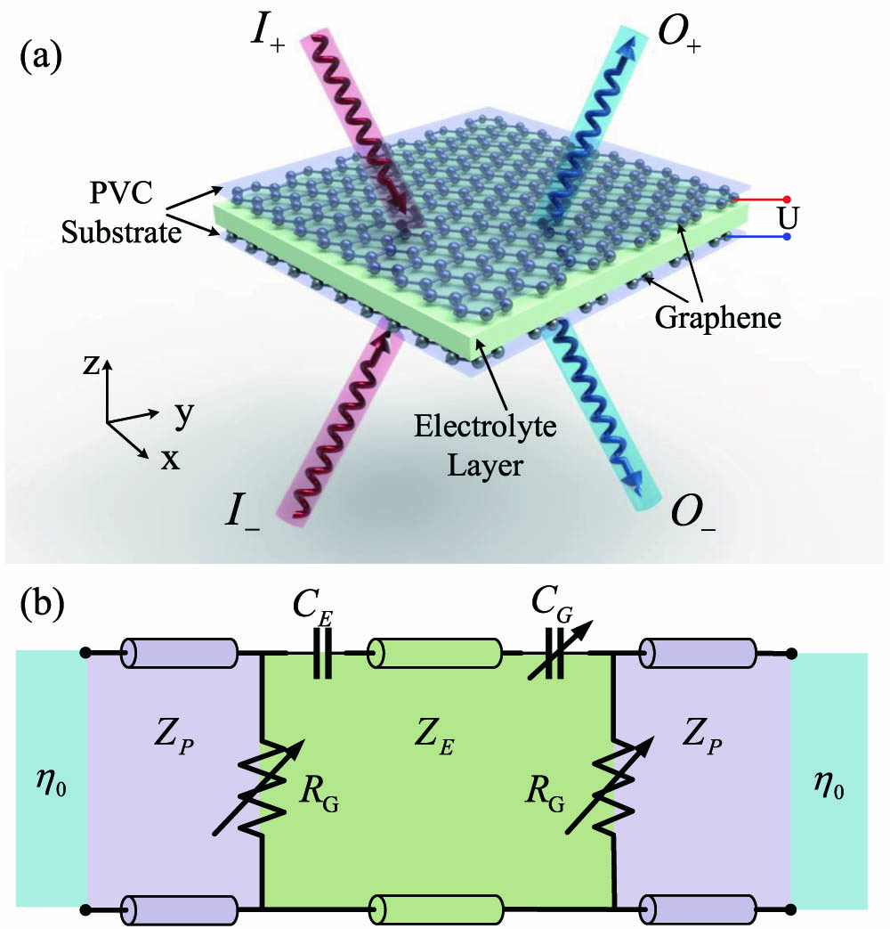
We propose and experimentally demonstrate the operation of an electrically tunable, broadband coherent perfect absorption (CPA) at microwave frequencies by harnessing the CPA features of a graphene–electrolyte–graphene sandwich structure (GSS). Using both a simplified lumped circuit model and full-wave numerical simulation, it is found that the microwave coherent absorptivity of the GSS can be tuned dynamically from nearly 50% to 100% by changing the Fermi level of the graphene. Strikingly, our simplified lumped circuit model agrees very well with the full-wave numerical model, offering valuable insight into the CPA operation of the device. The angle dependency of coherent absorption in the GSS is further investigated, making suggestions for achieving CPA at wide angles up to 80°. To show the validity and accuracy of our theory and numerical simulations, a GSS prototype is fabricated and measured in a C-band waveguide system. The reasonably good agreement between the experimental and the simulated results confirms that the tunable coherent absorption in GSS can be electrically controlled by changing the Fermi level of the graphene.
Photonics Research
2019, 7(8): 08000868
Author Affiliations
Abstract
1 Institute of Optics and Electronics, Chinese Academy of Sciences, Chengdu 610209, China
2 School of Mechanical Engineering, Southwest Jiaotong University, Chengdu 610031, China
3 University of Chinese Academy of Sciences, Beijing 100049, China
4 e-mail: shilifang@ioe.ac.cn
5 e-mail: dengqiling@ioe.ac.cn
This paper presents a method to design a monolithic complete-light modulator (MCLM) that fully controls the amplitude, phase, and polarization of incident light. The MCLM is made of birefringent materials that provide different refractive indices to orthogonal eigen-polarizations, the ordinary o and extraordinary e states. We propose an optimization method to calculate the two relief depth distributions for the two eigen-polarizations. Also, a merging algorithm is proposed to combine the two relief depth distributions into one. The corresponding simulations were carried out in this work and the desired light distribution, including information on amplitude, phase, and four polarization states, was obtained when a laser beam passed through a 16-depth-level micro-structure whose feature size is 8 μm. The structure was fabricated by common photolithography. An experimental optical system was also set up to test the optical effects and performances of the MCLM. The experimental performance of the MCLM agrees with the simulation results, which verifies the validity of the algorithms we propose in this paper.
Photonics Research
2019, 7(8): 08000875
Author Affiliations
Abstract
1 State Key Laboratory of Precision Measurement Technology & Instruments, Department of Precision Instrument, Tsinghua University, Beijing 100084, China
2 Department of Physics, 366 Le Conte Hall MS 7300, University of California, Berkeley, California 94720, USA
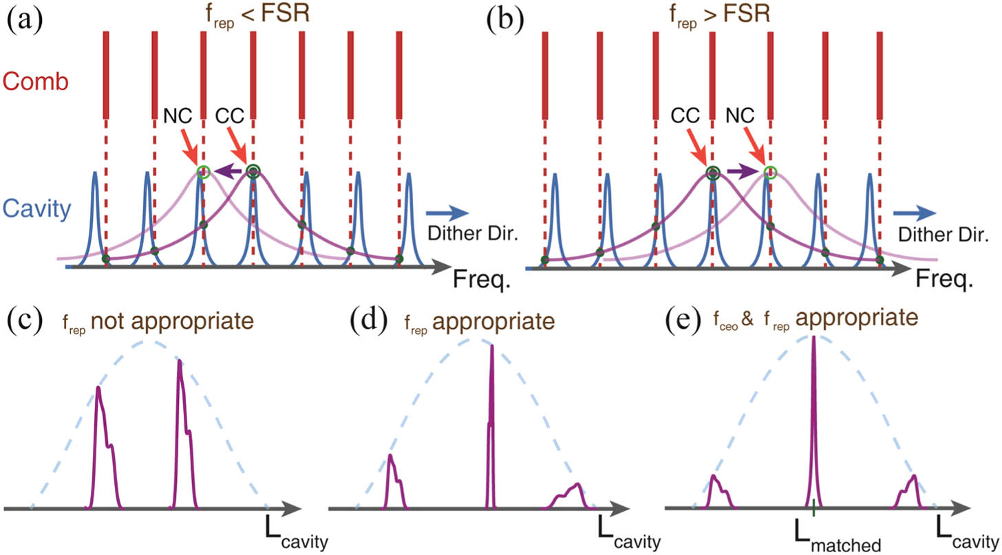
Resolution and bandwidth are critical for cavity-enhanced dual-comb spectroscopy (CE-DCS). Here, we pioneer an adaptive approach in CE-DCS to improve the broadband as well as the resolution. Postcorrections to dual-comb interferograms adaptively compensate the relative phase jitters of the optical frequency combs and result in both a mode-resolved spectral resolution and a signal-to-noise ratio of 440:1 in 1 s. Meanwhile, an adaptive comb-cavity locking scheme exploits more than 90% of the comb modes, covering 340 cm 1 (10 THz) at 6450 cm 1. For a single dual-comb interferogram, more than 40,000 comb teeth spaced by 250 MHz are measured in less than 7.5 ms, contributing to a noise equivalent absorption per spectral element of 2×10 10 cm 1 ·Hz 1/2. This adaptive cavity-enhanced dual-comb spectroscopy technique provides an attractive spectroscopic tool that may be utilized in trace-gas sensing, breath and cancer analysis, and engine combustion diagnosis.
Photonics Research
2019, 7(8): 08000883
Yao Fan 1,2,3†Jiasong Sun 1,2,3†Qian Chen 1,2,5Xiangpeng Pan 1,2,3[ ... ]Chao Zuo 1,2,3,*
Author Affiliations
Abstract
1 School of Electronic and Optical Engineering, Nanjing University of Science and Technology, Nanjing 210094, China
2 Jiangsu Key Laboratory of Spectral Imaging & Intelligent Sense, Nanjing University of Science and Technology, Nanjing 210094, China
3 Smart Computational Imaging (SCI) Laboratory, Nanjing University of Science and Technology, Nanjing 210094, China
4 Department of Electrical and Computer Engineering, Boston University, Boston, Massachusetts 02215, USA
5 e-mail: chenqian@njust.edu.cn
Differential phase contrast microscopy (DPC) provides high-resolution quantitative phase distribution of thin transparent samples under multi-axis asymmetric illuminations. Typically, illumination in DPC microscopic systems is designed with two-axis half-circle amplitude patterns, which, however, result in a non-isotropic phase contrast transfer function (PTF). Efforts have been made to achieve isotropic DPC by replacing the conventional half-circle illumination aperture with radially asymmetric patterns with three-axis illumination or gradient amplitude patterns with two-axis illumination. Nevertheless, the underlying theoretical mechanism of isotropic PTF has not been explored, and thus, the optimal illumination scheme cannot be determined. Furthermore, the frequency responses of the PTFs under these engineered illuminations have not been fully optimized, leading to suboptimal phase contrast and signal-to-noise ratio for phase reconstruction. In this paper, we provide a rigorous theoretical analysis about the necessary and sufficient conditions for DPC to achieve isotropic PTF. In addition, we derive the optimal illumination scheme to maximize the frequency response for both low and high frequencies (from 0 to 2NAobj) and meanwhile achieve perfectly isotropic PTF with only two-axis intensity measurements. We present the derivation, implementation, simulation, and experimental results demonstrating the superiority of our method over existing illumination schemes in both the phase reconstruction accuracy and noise-robustness.
Photonics Research
2019, 7(8): 08000890
Author Affiliations
Abstract
Department of Materials Science and State Key Laboratory of ASIC and System, Fudan University, Shanghai 200433, China
Optical microcavities, which support whispering gallery modes, have attracted tremendous attention in both fundamental research and potential applications. The emerging of two-dimensional materials offers a feasible solution to improve the performance of traditional microcavity-based optical devices. Besides, the integration of two-dimensional materials with microcavities will benefit the research of heterogeneous materials on novel devices in photonics and optoelectronics, which is dominated by the strongly enhanced light–matter interaction. This review focuses on the research of heterogeneous two-dimensional-material whispering-gallery-mode microcavities, opening a myriad of lab-on-chip applications, such as optomechanics, quantum photonics, comb generation, and low-threshold microlasing.
Photonics Research
2019, 7(8): 08000905
Author Affiliations
Abstract
1 CREOL, The College of Optics & Photonics, University of Central Florida, Orlando, Florida 32816-2700, USA
2 Changchun University of Science and Technology, Changchun 130012, China
3 e-mail: li@ucf.edu
We propose a mode demultiplexing hybrid (MDH) that integrates mode demultiplexing, local oscillator power splitting, and optical 90-deg mixing using multi-plane light conversion (MPLC). We demonstrate the realization of a three-mode MDH using four phase plates, one more than what is required for an MPLC-based mode demultiplexer, via numerical simulations. The performance of the three-mode MDH is comparable to that of commercial single-mode 90-deg hybrids. This multiple-functionality device enables simplification of the coherent optical front end of mode-division multiplexing receivers.
Photonics Research
2019, 7(8): 08000917
Author Affiliations
Abstract
1 Mork Family Department of Chemical Engineering and Materials Science, University of Southern California, Los Angeles, California 90089, USA
2 Ming Hsieh Department of Electrical Engineering-Electrophysics, University of Southern California, Los Angeles, California 90089, USA
Raman lasers based on integrated silica whispering gallery mode resonant cavities have enabled numerous applications from telecommunications to biodetection. To overcome the intrinsically low Raman gain value of silica, these devices leverage their ultrahigh quality factors (Q), allowing submilliwatt stimulated Raman scattering (SRS) lasing thresholds to be achieved. A closely related nonlinear behavior to SRS is stimulated anti-Stokes Raman scattering (SARS). This nonlinear optical process combines the pump photon with the SRS photon to generate an upconverted photon. Therefore, in order to achieve SARS, the efficiency of the SRS process must be high. As a result, achieving SARS in on-chip resonant cavities has been challenging due to the low lasing efficiencies of these devices. In the present work, metal-doped ultrahigh Q (Q>107) silica microcavity arrays are fabricated on-chip. The metal-dopant plays multiple roles in improving the device performance. It increases the Raman gain of the cavity material, and it decreases the optical mode area, thus increasing the circulating intensity. As a result, these devices have SRS lasing efficiencies that are over 10× larger than conventional silica microcavities while maintaining low lasing thresholds. This combination enables SARS to be generated with submilliwatt input powers and significantly improved anti-Stokes Raman lasing efficiency.
Photonics Research
2019, 7(8): 08000926
Yingshuang Shan 1Le Zhang 1,2,3,6,*Tianyuan Zhou 1,2Cen Shao 1[ ... ]Hao Chen 1,7,*
Author Affiliations
Abstract
1 Jiangsu Key Laboratory of Advanced Laser Materials and Devices, School of Physics and Electronic Engineering, Jiangsu Normal University, Xuzhou 221116, China
2 Department of Physics and Astronomy, Bowling Green State University, Bowling Green, Kentucky 43403, USA
3 School of Materials Science and Engineering, Georgia Institute of Technology, Atlanta, Georgia 30332, USA
4 SUSTech Academy for Advanced Interdisciplinary Studies, Southern University of Science and Technology, Shenzhen 518055, China
5 School of Mechanical Engineering, Jiangsu University, Zhenjiang 212013, China
6 e-mail: njutzl@163.com
7 e-mail: chenhao@jsnu.edu.cn
The Cr4+-doped yttrium aluminum garnet (Cr4+:YAG) saturable absorber, a new generation of passively Q-switched solid-state laser material, faces a significant obstacle of low conversion rate of chromium from trivalent to tetravalent, degrading efficiency in a passively Q-switched laser. In this paper, highly transparent Cr4+:YAG ceramics were fabricated and committed to compare the laser performance with Cr4+:YAG crystals on a 1 μm passively Q-switched laser. Thanks to the grain boundary effect, the Cr4+ conversion efficiency of 0.05 at.% Cr4+:YAG transparent ceramics coated with high transparency (HT) films (T=86.46% at 1064 nm) was nine times higher than that of 0.1 at.% Cr4+:YAG single crystals coated with HT films (T=84.00% at 1064 nm). Differing from the counterpart Cr4+:YAG crystals, no absorption saturation tendency was observed for the 0.05 at.% Cr:YAG ceramics when the pump power exceeded 1900 mW. Furthermore, the repetition frequency reached 217 kHz for 0.05 at.% Cr:YAG ceramics, which was a three-fold factor increase from that of the corresponding single crystal. The advantages of transparent ceramics over single crystals were proved through laser performance for the first time, to the best of our knowledge. This study also provided compelling evidence for replacing single crystals with ceramics for u
Photonics Research
2019, 7(8): 08000933
Author Affiliations
Abstract
1 College of Optical Sciences, University of Arizona, Tucson, Arizona 85721, USA
2 State Key Laboratory of Information Photonics and Optical Communications, Beijing University of Posts and Telecommunications, Beijing 100876, China
3 Department of Biomedical Engineering, University of Arizona, Tucson, Arizona 85721, USA
Whispering gallery mode (WGM) microtoroid optical resonators have been effectively used to sense low concentrations of biomolecules down to the single molecule limit. Optical WGM biochemical sensors such as the microtoroid operate by tracking changes in resonant frequency as particles enter the evanescent near field of the resonator. Previously, gold nanoparticles have been coupled to WGM resonators to increase the magnitude of resonance shifts via plasmonic enhancement of the electric field. However, this approach results in increased scattering from the WGM, which degrades its quality (Q) factor, making it less sensitive to extremely small frequency shifts caused by small molecules or protein conformational changes. Here, we show using simulation that precisely positioned trimer gold nanostructures generate dark modes that suppress radiation loss and can achieve high (>106) Q with an electric-field intensity enhancement of 4300, which far exceeds that of a single rod (2500 times). Through an overall evaluation of a combined enhancement factor, which includes the Q factor of the system, the sensitivity of the trimer system was improved 105× versus 84× for a single rod. Further simulations demonstrate that unlike a single rod system, the trimer is robust to orientation changes and has increased capture area. We also conduct stability tests to show that small positioning errors do not greatly impact the result.
Photonics Research
2019, 7(8): 08000939
Author Affiliations
Abstract
1 School of Physics and Astronomy, State Key Laboratory of Advanced Optical Communication Systems and Networks, Shanghai Jiao Tong University, Shanghai 200240, China
2 Synergetic Innovation Center of Quantum Information and Quantum Physics, University of Science and Technology of China, Hefei 230026, China
Quantum communication has been rapidly developed due to its unconditional security and successfully implemented through optical fibers and free-space air in experiments. To build a complete quantum communication network involving satellites in space and submersibles in ocean, the underwater quantum channel has been investigated in both theory and experiment. However, the question of whether the polarization encoded qubit can survive through a long-distance and high-loss underwater channel, which is considered as the restricted area for satellite-borne radio waves, still remains. Here, we experimentally demonstrate the transmission of blue-green photonic polarization states through 55-m-long water. We prepare six universal quantum states at the single photon level and observe their faithful transmission in a large marine test platform. We obtain complete information of the channel by quantum process tomography. The distance demonstrated in this work reaches a region allowing potential real applications, representing a step further towards air-to-sea quantum communication.
Photonics Research
2019, 7(8): 08000A40
Weizong Xu 1,2,*†Yating Shi 1†Fangfang Ren 1Dong Zhou 1[ ... ]Hai Lu 1,3,*
Author Affiliations
Abstract
1 School of Electronic Science and Engineering, Nanjing University, Nanjing 210023, China
2 e-mail: wz.xu@nju.edu.cn
3 e-mail: hailu@nju.edu.cn
In this work, a GaN p-i-n diode based on Mg ion implantation for visible-blind UV detection is demonstrated. With an optimized implantation and annealing process, a p-GaN layer and corresponding GaN p-i-n photodiode are achieved via Mg implantation. As revealed in the UV detection characterizations, these diodes exhibit a sharp wavelength cutoff at 365 nm, high UV/visible rejection ratio of 1.2×10⁴, and high photoresponsivity of 0.35 A/W, and are proved to be comparable with commercially available GaN p-n photodiodes. Additionally, a localized states-related gain mechanism is systematically investigated, and a relevant physics model of electric-field-assisted photocarrier hopping is proposed. The demonstrated Mg ion-implantation-based approach is believed to be an applicable and CMOS-process-compatible technology for GaN-based p-i-n photodiodes.
Photonics Research
2019, 7(8): 08000B48
Author Affiliations
Abstract
UV Craftory Co., Ltd., 2-305, Fujimidai 2-7-2, Chikusa-ku, Nagoya 464-0015, Japan
This paper reviews and introduces the techniques for boosting the light-extraction efficiency (LEE) of AlGaN-based deep-ultraviolet (DUV: λ<300 nm) light-emitting diodes (LEDs) on the basis of the discussion of their molecular structures and optical characteristics, focusing on organoencapsulation materials. Comparisons of various fluororesins, silicone resin, and nonorgano materials are described. The only usable organomaterial for encapsulating DUV-LEDs is currently considered to be polymerized perfluoro(4-vinyloxy-1-butene) (p-BVE) terminated with a CF3 end group. By forming hemispherical lenses on DUV-LED dies using p-BVE having a CF3 end group with a refractive index of about 1.35, the LEE was improved by 1.5-fold, demonstrating a cost-feasible packaging technique.
Photonics Research
2019, 7(8): 08000B55