1 Shanghai Advanced Research Institute, Chinese Academy of Sciences, Shanghai 201210, China
2 Center for Terahertz Waves and College of Precision Instrument and Optoelectronics Engineering, Key Laboratory of Opto-electronics Information and Technical Science, Ministry of Education, Tianjin University, Tianjin 300072, China
3 University of Chinese Academy of Sciences, Beijing 100049, China
4 ShanghaiTech University, Shanghai 201210, China
5 e-mail: zhangyz@sari.ac.cn
6 e-mail: yantm@sari.ac.cn
7 e-mail: jiangyh@sari.ac.cn
The origin of terahertz (THz) generation in a gas-phase medium is still in controversy, although the THz sources have been applied across many disciplines. Herein, the THz generation in a dual-color field is investigated experimentally by precisely controlling the relative phase and polarization of dual-color lasers, where the accompanying third-harmonic generation is employed for in situ determination of the relative phase up to sub-wavelength accuracy. Joint studies with the strong approximation (SFA) theory reveal that the continuum-continuum (CC) transition within an escaped electron wave packet in the single atom gives birth to THz emission, without the necessity of considering the plasma effect. Meanwhile, we develop the analytic form from SFA-based CC description, which is able to reproduce and decompose the classical photocurrent model from the viewpoint of microscopic quantum theory, establishing the quantum-classical correspondence and bringing a novel insight into the mechanism of THz generation. Present studies leave open the possibility for probing the ultrafast dynamics of continuum electrons and a new dimension for the study of THz-related science and methodology.
1 Beijing Key Laboratory of Nanophotonics and Ultrafine Optoelectronic Systems, School of Physics, Beijing Institute of Technology, Beijing 100081, China
2 Beijing Engineering Research Center of Mixed Reality and Advanced Display, School of Optics and Photonics, Beijing Institute of Technology, Beijing 100081, China
3 AICFVE of Beijing Film Academy, Beijing 100088, China
4 e-mail: liusir@bit.edu.cn
Lead halide perovskites have drawn extensive attention over recent decades owing to their outstanding photoelectric performances. However, their toxicity and instability are big issues that need to be solved for further commercialization. Herein, we adopt a facile dry ball milling method to synthesize lead-free (, Cl) perovskites with photoluminescence (PL) quantum yield up to 60%. The optical features including broad emission spectrum, large Stokes shift, and long PL lifetime can be attributed to self-trapped exciton recombination. The as-synthesized blue emissive and green emissive lead-free perovskite powders have good thermal stability and photostability. Furthermore, UV-pumped phosphor-converted light-emitting diodes were obtained by using and as phosphors.
1 Aston Institute of Photonics Technologies, Aston University, Aston Triangle, Birmingham B4 7ET, UK
2 Leibniz Institute of Photonics Technology, Albert-Einstein srt. 9, Jena 07745, Germany
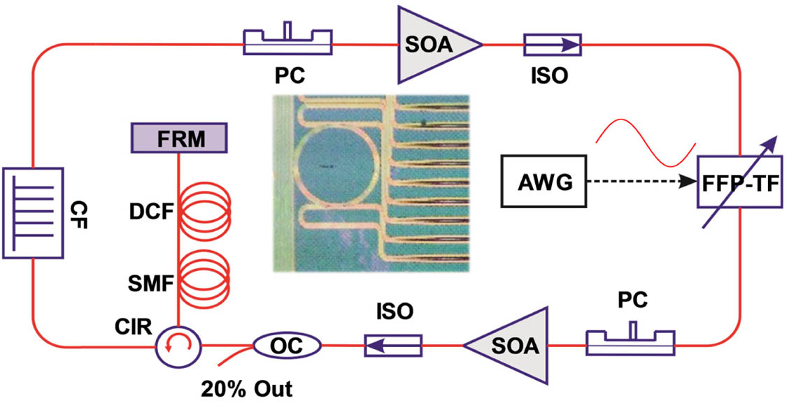
Bidirectional ultrafast fiber lasers present an attractive solution, enabling the generation of two mutually coherent ultrashort pulse trains in a simple and turnkey system. Still, the lack of a comprehensive numerical model describing steady-state bidirectional generation, and even less ultrafast soliton breakdowns and collisions, is obstructing the achievement of the performance compared with unidirectional lasers. In this paper, we have experimentally investigated real-time build-up dynamics of counter-propagating solitons in an ultrafast ring Er-doped fiber laser via the dispersive Fourier transform methodology. We parade that counter-propagating pulses experience independent build-up dynamics from modulation instability, undergoing breathing dynamics and diverging subordinate pulse structure formation and annihilation to a stable bidirectional pulse train. Yet, the interaction of pulses in the cavity presents the key underlying phenomenon driving formation evolution distinct from unidirectional pulse build-up. Our findings will provide physical foundations for bidirectional ultrafast fiber laser design to carry forward their application.
1 Key Laboratory for Quantum Optics, Shanghai Institute of Optics and Fine Mechanics, Chinese Academy of Sciences, Shanghai 201800, China
2 Guangdong Provincial Key Laboratory of Quantum Engineering and Quantum Materials, SPTE, South China Normal University, Guangzhou 510006, China
3 School of Mathematics and Physics, Jiangsu University of Science and Technology, Zhenjiang 212003, China
A mixed light field generated from a two-level atomic ensemble can be used for two-photon interference. In this mixed light field, correlated paired photons generated from a four-wave mixing process provide a signal of two-photon interference, while Rayleigh scattered photons of the pump laser provide a stable reference to calibrate the normalized second-order correlation function. We demonstrate two-photon interference using the Hong–Ou–Mandel and Hanbury Brown–Twiss interferometers. A direct quantitative comparison between theoretical predictions and experimental data is performed under perturbed experimental conditions, which reveal this kind of light source has potential application for quantum metrology.
1 Department of Physics and Astronomy, Aarhus University, Ny Munkegade 120, DK-8000 Aarhus C, Denmark
2 Peter Grünberg Institute 9 (PGI 9), Forschungszentrum Jülich, 52425 Jülich, Germany
3 JARA-Institut Green IT, RWTH Aachen, Germany
4 DTU Fotonik, Technical University of Denmark, Frederiksborgvej 399, DK-4000 Roskilde, Denmark
5 Pollard Institute, School of Electronic and Electrical Engineering, University of Leeds, Leeds, UK
We present an experimental setup capable of time-resolved photoluminescence spectroscopy for photon energies in the range of 0.51 to 0.56 eV with an instrument time response of 75 ps. The detection system is based on optical parametric three-wave mixing, operates at room temperature, has spectral resolving power, and is shown to be well suited for investigating dynamical processes in germanium-tin alloys. In particular, the carrier lifetime of a direct-bandgap film with concentration and biaxial strain is determined to be at a temperature of 20 K. A room-temperature investigation indicates that the variation in this lifetime with temperature is very modest. The characteristics of the photoluminescence as a function of pump fluence are discussed.
1 College of Materials Science and Engineering, Shenzhen University, Shenzhen 518060, China
2 State Key Laboratory of Functional Materials for Informatics, Shanghai Institute of Microsystem and Information Technology, Chinese Academy of Sciences, Shanghai 200050, China
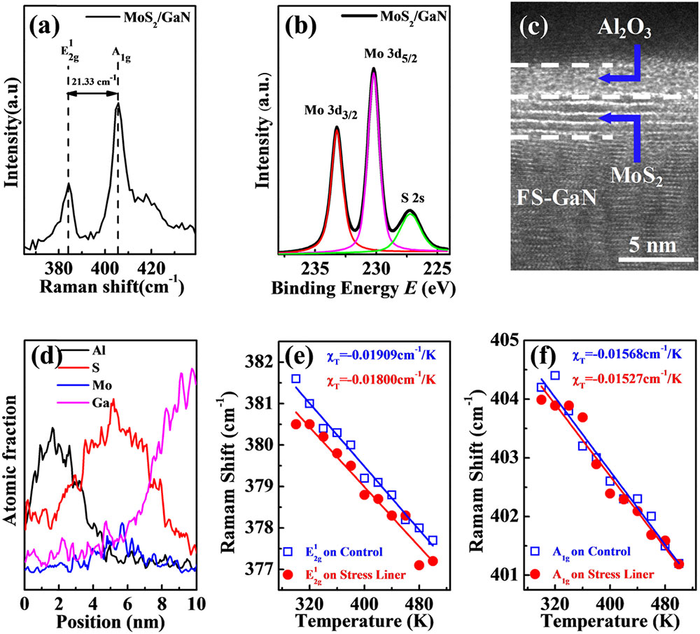
Strain regulation as an effective way to enhance the photoelectric properties of two-dimensional (2D) transition metal dichalcogenides has been widely employed to improve the performance of photovoltaic devices. In this work, tensile strain was introduced in multilayer grown on GaN by depositing 3 nm of on the surface. The temperature-dependent Raman spectrum shows that the thermal stability of is improved by . Theoretical simulations confirmed the existence of tensile strain on covered with , and the bandgap and electron effective mass of six layers of decreased due to tensile strain, which resulted in an increase of electron mobility. Due to the tensile strain effect, the photodetector with the stress liner achieved better performance under the illumination of 365 nm wavelength, including a higher responsivity of 24.6 A/W, photoconductive gain of 520, and external quantum efficiency of 8381%, which are more than twice the corresponding values of photodetectors without . Our work provides an effective technical way for improving the performance of 2D material photodetectors.
1 Shaanxi Provincial Key Laboratory of Photonics & Information Technology, Xi’an Jiaotong University, Xi’an 710049, China
2 Solid-State Lighting Engineering Research Center, Xi’an Jiaotong University, Xi’an 710049, China
A full structure 290-nm ultraviolet light-emitting diode (UV-LED) with a nanoporous n-AlGaN underlayer was fabricated by top via hole formation followed by high-voltage electrochemical etching. The 20 to 120 nm nanopores were prepared in regular doped n-AlGaN by adjusting the etching voltage. The comparison between the Raman spectrum and the photoluminescence wavelength shows that the biaxial stress in the nanoporous material is obviously relaxed. The photoluminescence enhancement was found to be highly dependent on the size of the pores. It not only improves the extraction efficiency of top-emitting transverse-electric (TE)-mode photons but also greatly improves the efficiency of side-emitting transverse-magnetic (TM)-mode photons. This leads to the polarization change of the side-emitting light from to . The intensity of the electroluminescence was increased by 36.5% at 100 mA, and the efficiency droop at high current was found to decrease from 61% to 31%.
1 Ningbo Institute of Materials Technology and Engineering, Chinese Academy of Sciences, Ningbo 315201, China
2 University of Chinese Academy of Sciences, Beijing 100049, China
3 College of Physics Science & Technology, Laboratory of Optoelectronic Materials and Detection Technology, Guangxi Key Laboratory for the Relativistic Astrophysics, Guangxi University, Nanning 530004, China
4 Advanced Micro-Fabrication Equipment Inc., Shanghai 201201, China
6 Advanced Semiconductor Laboratory, King Abdullah University of Science and Technology (KAUST), Thuwal 23955, Saudi Arabia
We report on the carrier dynamic and electronic structure investigations on AlGaN-based deep-ultraviolet multiple quantum wells (MQWs) with lateral polarity domains. The localized potential maximum is predicted near the domain boundaries by first-principle calculation, suggesting carrier localization and efficient radiative recombination. More importantly, lateral band diagrams of the MQWs are proposed based on electron affinities and valance band levels calculated from ultraviolet (UV) photoelectron spectroscopy. The proposed lateral band diagram is further demonstrated by surface potential distribution collected by Kelvin probe microscopy and the density-of-state calculation of energy bands. This work illustrates that lateral polarity structures are playing essential roles in the electronic properties of III-nitride photonic devices and may provide novel perspective in the realization of high-efficiency UV emitters.
Department of Opto-Electronics, Sichuan University, Chengdu 610065, China
Fringe projection profilometry has been increasingly sought and applied in dynamic three-dimensional (3D) shape measurement. In this work, a robust, high-efficiency 3D measurement based on Gray-coded light is proposed. Unlike the traditional method, a tripartite phase unwrapping method is proposed to avoid the jump errors on the boundary of code words, which are mainly caused by the defocusing of the projector and the motion of the tested object. Subsequently, the time-overlapping coding strategy is presented to greatly increase the coding efficiency, decreasing the projected number in each group from seven (i.e., ) to four (i.e., ) for one restored 3D frame. The combination of two proposed techniques allows the reconstruction of a pixel-wise and unambiguous 3D geometry of dynamic scenes with strong noise using every four projected patterns. To the best of our knowledge, the presented techniques for the first time preserve the high anti-noise ability of a method based on the Gray code while overcoming the drawbacks of jump errors and low coding efficiency. Experiments have demonstrated that the proposed method can achieve robust, high-efficiency 3D shape measurement of high-speed dynamic scenes even polluted by strong noise.
1 Terahertz Technology Innovation Research Institute, Terahertz Spectrum and Imaging Technology Cooperative Innovation Center, Shanghai Key Laboratory of Modern Optical System, University of Shanghai for Science and Technology, Shanghai 200093, China
2 Shanghai Institute of Intelligent Science and Technology, Tongji University, Shanghai 200092, China
3 e-mail: ymzhu@usst.edu.cn
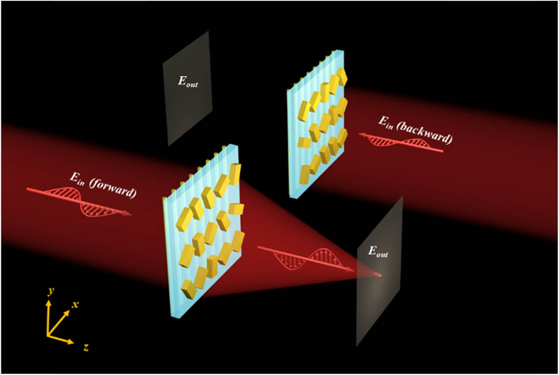
Asymmetric transmission, defined as the difference between the forward and backward transmission, enables a plethora of applications for on-chip integration and telecommunications. However, the traditional method for asymmetric transmission is to control the propagation direction of the waves, hindering further applications. Metasurfaces, a kind of two-dimensional metamaterials, have shown an unprecedented ability to manipulate the propagation direction, phase, and polarization of electromagnetic waves. Here we propose and experimentally demonstrate a metasurface-based directional device consisting of a geometric metasurface with spatially rotated microrods and metallic gratings, which can simultaneously control the phase, polarization, and propagation direction of waves, resulting in asymmetric focusing in the terahertz region. These dual-layered metasurfaces for asymmetric focusing can work in a wide bandwidth ranging from 0.6 to 1.1 THz. The flexible and robust approach for designing broadband asymmetric focusing may open a new avenue for compact devices with potential applications in encryption, information processing, and communication.
1 Max Planck Institute for the Science of Light, Staudtstraße. 2, 91058 Erlangen, Germany
2 Department of Physics, Friedrich-Alexander-Universität, Staudtstraße. 2, 91058 Erlangen, Germany
Laser cooling of mechanical degrees of freedom is one of the most significant achievements in the field of optomechanics. Here, we report, for the first time to the best of our knowledge, efficient passive optomechanical cooling of the motion of a freestanding waveguide coupled to a whispering-gallery-mode (WGM) resonator. The waveguide is an 8 mm long glass-fiber nanospike, which has a fundamental flexural resonance at and a -factor of . Upon launching laser power at an optical frequency close to the WGM resonant frequency, we observed cooling of the nanospike resonance from room temperature down to 1.8 K. Simultaneous cooling of the first higher-order mechanical mode is also observed. The strong suppression of the overall Brownian motion of the nanospike, observed as an 11.6 dB reduction in its mean square displacement, indicates strong optomechanical stabilization of linear coupling between the nanospike and the cavity mode. The cooling is caused predominantly by a combination of photothermal effects and optical forces between nanospike and WGM resonator. The results are of direct relevance in the many applications of WGM resonators, including atom physics, optomechanics, and sensing.
1 Centre for Optical and Electromagnetic Research, State Key Laboratory for Modern Optical Instrumentation, Zhejiang Provincial Key Laboratory for Sensing Technologies, Zhejiang University, Hangzhou 310058, China
2 Institute of Port, Coastal and Offshore Engineering, Ocean College, Zhejiang University, Zhoushan 316021, China
3 Engineering Research Center of Oceanic Sensing Technology and Equipment, Ministry of Education, Zhejiang University, Hangzhou 310000, China
4 e-mail: leimeng.zhuang@ieee.org
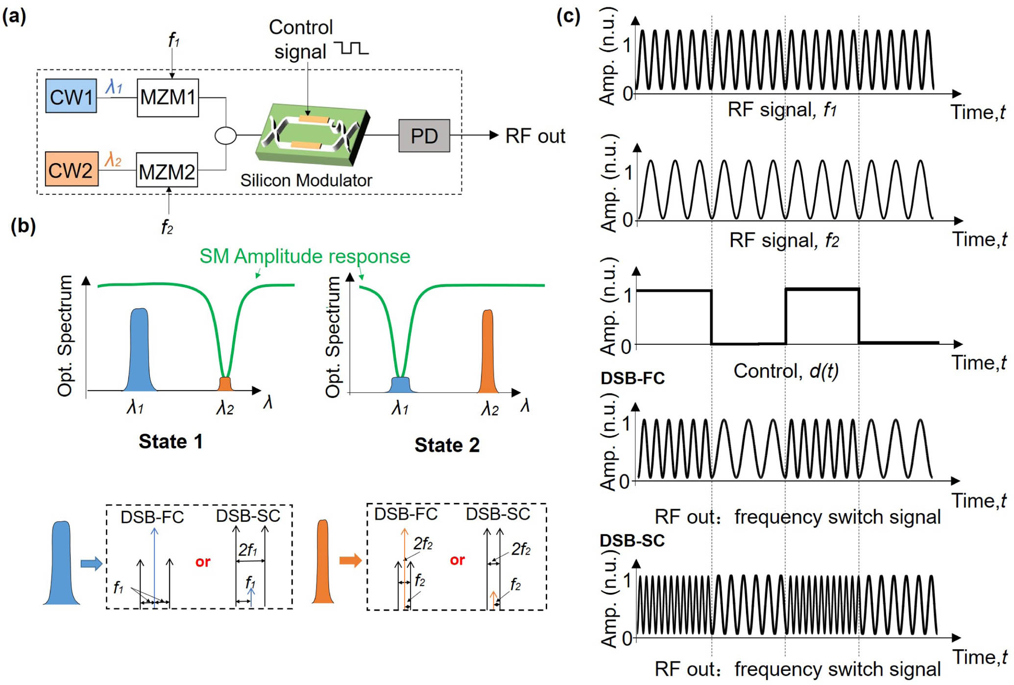
Radio frequency (RF) switches are essential for implementing routing of RF signals. However, the increasing demand for RF signal frequency and bandwidth is posing a challenge of switching speed to the conventional solutions, i.e., the capability of operating at a sub-nanosecond speed or faster. In addition, signal frequency reconfigurability is also a desirable feature to facilitate new innovations of flexible system functions. Utilizing microwave photonics as an alternative path, we present here a photonic implementation of an RF switch providing not only the capability of switching at a sub-nanosecond speed but also options of frequency doubling of the input RF signals, allowing for flexible output waveforms. The core device is a traveling-wave silicon modulator with a device size of and a modulation bandwidth of 10 GHz. Using microwave frequencies, i.e., 15 GHz and 20 GHz, as two simultaneous RF input signals, we experimentally demonstrated their amplitude and frequency switching as well as that of the doubled frequencies, i.e., 30 GHz and 40 GHz, at a switching frequency of 5 GHz. The results of this work point to a solution for creating high-speed RF switches with high compactness and flexibility.
1 Laboratoire de Physique de l’Ecole normale supérieure, ENS, Université PSL, CNRS, Sorbonne Université, Université de Paris, F-75005 Paris, France
2 i2S, 28-30 rue Jean Perrin 33608 Pessac, France
3 Centre de Nanosciences et de Nanotechnologies (C2N), CNRS UMR 9001, Université Paris-Saclay, 91120 Palaiseau, France
4 Currently at: Institut d’Electronique et des Systèmes, CNRS (UMR 5214), Univ Montpellier, 860 rue de Saint-Priest, 34 095 Montpellier Cedex 5, France
Optically driven photoconductive switches are one of the predominant sources currently used in terahertz imaging systems. However, owing to their low average powers, only raster-based images can be taken, resulting in slow acquisition. In this work, we show that by placing a photoconductive switch within a cavity, we are able to generate absolute average THz powers of 181 μW with the frequency of the THz emission centered at 1.5 THz—specifications ideally adapted to applications such as non-destructive imaging. The cavity is based on a metal–insulator–metal structure that permits an enhancement of the average power by almost 1 order of magnitude compared to a standard structure, while conserving a broadband spectral response. We demonstrate proof-of-principle real-time imaging using this source, with the broadband spectrum permitting to eliminate strong diffraction artifacts.
Department of Electrical and Computer Engineering, Centre for Optics, Photonics and Laser (COPL), Université Laval, Québec, Québec G1V 0A6, Canada
Wavelength-dependent polarization state of light carries crucial information about light–matter interactions. However, its measurement is limited to bulky, high energy-consuming devices, which prohibits many modern, portable applications. Here, we propose and demonstrate a chip-scale spectropolarimeter implemented using a complementary metal oxide semiconductor compatible silicon photonics technology. Four compact Vernier microresonator spectrometers are monolithically integrated with a broadband polarimeter consisting of a 2D nanophotonic antenna and a polarimetric circuit to achieve full-Stokes spectropolarimetric analysis. The proposed device offers a solid-state spectropolarimetry solution with a small footprint of 1 mm × 0.6 mm and low power consumption of 360 mW. Full-Stokes spectral detection across a broad spectral range of 50 nm with a resolution of 1 nm is demonstrated in characterizing a material possessing structural chirality. The proposed device may enable a broader application of spectropolarimetry in the fields ranging from biomedical diagnostics and chemical analysis to observational astronomy.
1 CAS Key Laboratory of Mechanical Behavior and Design of Materials, Department of Precision Machinery and Precision Instrumentation, University of Science and Technology of China, Hefei 230027, China
2 e-mail: jwl@ustc.edu.cn
3 e-mail: dongwu@ustc.edu.cn
Manipulating Airy beams to symmetric Airy beams (SABs) with abruptly autofocusing and self-accelerating properties has attracted much attention. With such a particular propagation dynamic, SABs may provide great potential in dynamic signal imaging. On the other hand, the generation of SABs by spatial light modulators suffers from the limitations of phase gradient accuracy, low optical efficiency (), and a bulky footprint. Therefore, exploring imaging applications and optimal generation methods of these Airy-type beams deserves further research. Here, based on the coordinate transformation of SAB, an asymmetric Airy beam (AAB) is realized. Symmetric/asymmetric cubic phase microplates (SCPPs/ACPPs) are designed and fabricated for generating SAB/AAB. The SCPP/ACPP demonstrates superior performance: compact construction (), continuous variation of phase, high efficiency ( at 532 nm), and broadband operation from 405 to 780 nm. Dynamic imaging under monochromatic and polychromatic lights is realized by the SAB/AAB, indicating various results at different propagation distances with a certain initial signal. Further investigation reveals that the SCPP on a soft substrate maintains its physical dimensions and optical properties unchanged during stretching. Our work enables wide potential applications in integrated optics, beam manipulation, and imaging.
2 School of Electrical and Electronic Engineering, Nanyang Technological University, Singapore 639798, Singapore
3 School of Optical and Electronic Information & Wuhan National Laboratory for Optoelectronics, Huazhong University of Science and Technology, Wuhan 430074, China
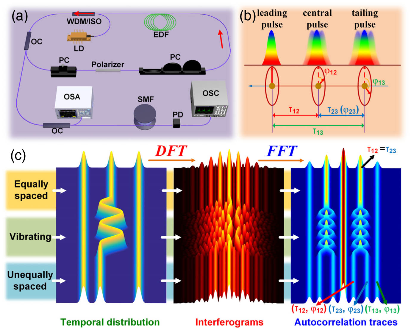
The evolution of soliton molecules emphasizes the complex soliton dynamics akin to matter molecules. Beyond the simplest soliton molecule—a soliton pair constituted by two bound pulses—soliton molecules with more constituents have more degrees of freedom because of the temporal pulse separations and relative phases. Here we detailedly characterize the transient dynamics of soliton triplets in fiber lasers by using the dispersive Fourier transform measurement. A particular form of leading, central, and tailing pulses is constructed to shed new light on more intriguing scenarios and fuel the molecular analogy. Especially the vibrating dynamics of the central and tailing pulses are captured near the regime of equally spaced soliton triplets, which is reminiscent of the recurrent timing jitters within multi-pulse structures. Further insights enable access into a universal form of unequally spaced soliton triplets interpreted as soliton molecules. Different binding strengths of intramolecular and intermolecular bonds are validated with respect to the diverse internal motions involved in this soliton triplet molecule. All these findings unveil the transient dynamics with more degrees of freedom as well as highlight the possible application for all-optical bit storage.
1 Key Laboratory of Photoelectronic Imaging Technology and System, School of Optics and Photonics, Beijing Institute of Technology, Beijing 100081, China
2 School of Computer Science and Information Security, Guilin University of Electronic Technology, Guilin 541004, China
3 Department of Electrical and Computer Engineering, University of Delaware, Newark, Delaware 19716, USA
4 e-mail: ciom_xtf1@bit.edu.cn
5 e-mail: maxu@bit.edu.cn
This publisher’s note corrects the authorship in Photon. Res.8, 395 (2020)PRHEIZ2327-912510.1364/PRJ.377665.
College of Physics and Information Engineering, Fuzhou University, Fuzhou 350108, China
Fluorescence fluctuation-based superresolution techniques can achieve fast superresolution imaging on a cost-effective wide-field platform at a low light level with reduced phototoxicity. However, the current methods exhibit certain imaging deficiencies that misinterpret nanoscale features reconstructed from fluctuating image sequences, thus degrading the superresolution imaging quality and performance. Here we propose cross-cumulant enhanced radiality nanoscopy (CERN), which employs cross-cumulant analysis in tandem with radiality processing. We demonstrated that CERN can significantly improve the spatial resolution at a low light level while eliminating the misinterpretations of nanoscale features of the existing fluctuation-based superresolution methods. In the experiment, we further verified the superior performance of CERN over the current methods through performing multicolor superresolution imaging of subcellular microtubule networks and clathrin-coated pits as well as the high-precision reconstruction of densely packed RNA transcripts.
1 State Key Laboratory on Integrated Optoelectronics, Institute of Semiconductors, Chinese Academy of Sciences, Beijing 100083, China
2 Center of Materials Science and Optoelectronics Engineering, University of Chinese Academy of Sciences, Beijing 100049, China
3 Beijing Academy of Quantum Information Sciences, Beijing 100193, China
A horizontal ridge waveguide emitter on a silicon (100) substrate with a multi-quantum-well (MQW) active layer was fabricated by molecular beam epitaxy. The device structure was designed to reduce light absorption of metal electrodes and improve injection efficiency. Electroluminescence (EL) at a wavelength of 2160 nm was observed at room temperature. Theoretical calculations indicate that the emission peak corresponds well to the direct bandgap transition (). The light output power was about 2.0 μW with an injection current density of . These results show that the horizontal GeSn/Ge MQW ridge waveguide emitters have great prospects for group-IV light sources.
1 Photonics Research Centre, Department of Electronic and Information Engineering, The Hong Kong Polytechnic University, Hong Kong SAR, China
2 The Hong Kong Polytechnic University Shenzhen Research Institute, Shenzhen 518057, China
3 Photonics Research Centre, Department of Electrical Engineering, The Hong Kong Polytechnic University, Hong Kong SAR, China
4 Department of Physics and Materials Science, City University of Hong Kong, Hong Kong SAR, China
Frequency comb swept lasers are the enabling technology of circular interferometric imaging, which was proposed to break the bottleneck of data acquisition and processing in optical coherence tomography (OCT) at video rate. In this paper, we propose and demonstrate a highly coherent frequency comb swept laser by using a high-quality (high-Q) microring comb filter to discretize a Fourier-domain mode-locked (FDML) laser. The microring filter has a Q factor of and a linewidth of . To demonstrate the improvement in performance, a Fabry–Pérot comb filter with a Q factor of and a linewidth of 3.1 GHz is also used in the experiment for comparison. Both comb filters have free spectral ranges (FSRs) of for consistence. Stable and clearly discretized temporal waveforms and frequency comb spectra with 50 GHz FSR are observed. Adoption of the high-Q microring filter narrows the instantaneous linewidth of the FDML laser down to 1.5 GHz. The OCT system with the frequency comb swept laser source with a microring filter demonstrates an ultralong imaging range, which has a 6, 10, and 15 dB sensitivity roll-off length of , , and over 100 mm, respectively.
1 Key Laboratory of Semiconductor Materials Science, Institute of Semiconductors, Chinese Academy of Sciences, Beijing 100083, China
2 Center of Materials Science and Optoelectronics Engineering, University of Chinese Academy of Sciences, Beijing 100049, China
3 Beijing R&D Institute, VanJee Technology, Beijing 100193, China
A SiN-Si dual-layer optical phased array (OPA) chip is designed and fabricated. It combines the low loss of SiN with the excellent modulation performance of Si, which improves the performance of Si single-layer OPA. A novel optical antenna and an improved phase modulation method are also proposed, and a two-dimensional scanning range of is achieved, which makes the OPA chip more practical.
Shenzhen International Graduate School, Tsinghua University, Shenzhen 518055, China
Prior-free imaging beyond the memory effect (ME) is critical to seeing through the scattering media. However, methods proposed to exceed the ME range have suffered from the availability of prior information of imaging targets. Here, we propose a blind target position detection for large field-of-view scattering imaging. Only exploiting two captured multi-target near-field speckles at different imaging distances, the unknown number and locations of the isolated imaging targets are blindly reconstructed via the proposed scaling-vector-based detection. Autocorrelations can be calculated for the speckle regions centered by the derived positions via low-cross-talk region allocation strategy. Working with the modified phase retrieval algorithm, the complete scene of the multiple targets exceeding the ME range can be reconstructed without any prior information. The effectiveness of the proposed algorithm is verified by testing on a real scattering imaging system.
1 Engineering Research Center of Molecular & Neuro Imaging, Ministry of Education, Xi’an 710126, China
2 School of Life Science and Technology, Xidian University, Xi’an 710126, China
3 School of Information Sciences and Technology, Northwest University, Xi’an 710127, China
4 Department of Electrical and Computer Engineering & Biomedical Engineering, Boston University, Boston, Massachusetts 02215, USA
Scattering is a huge challenge for microscopic imaging. Indeed, it is difficult to observe target chemicals in scattering media by means of the current Gaussian beam-based stimulated Raman scattering (SRS) microscopy, since the tight focus of the Gaussian beam is destroyed after propagating through a certain distance. Bessel beams, featuring self-reconstructing property, may bring a solution to this problem. By combining Bessel beams with SRS microscopy, we can probe the SRS signal from a scattering medium. In this paper, using the beam propagation method, we first simulate the propagation of the Bessel beam as well as the generation and self-reconstruction of SRS signals. By adding glass beads along the beam propagation path in order to simulate scattering, the propagation of the Bessel beams and the generation of the SRS signals will change. Then, we design a series of simulations to investigate the influence of the size, position, number, and distribution of the added glass beads on the generation of the SRS signals. A preliminary experiment is also carried out to confirm the simulation predictions. Results demonstrate that the SRS signals can be generated or be recovered at a certain depth in scattering media, and that such signals are greatly affected by the parameters of the scatters.
1 Department of Automation, Tsinghua University, Beijing 100084, China
2 Institute for Brain and Cognitive Science, Tsinghua University, Beijing 100084, China
3 Tsinghua Shenzhen International Graduate School, Tsinghua University, Shenzhen 518055, China
4 Beijing Innovation Center for Future Chip, Tsinghua University, Beijing 100084, China
5 Institute of Microelectronics, Tsinghua University, Beijing 100084, China
6 Beijing National Research Center for Information Science and Technology, Tsinghua University, Beijing 100084, China
7 e-mail: lin-x@tsinghua.edu.cn
8 e-mail: qhdai@tsinghua.edu.cn
Training an artificial neural network with backpropagation algorithms to perform advanced machine learning tasks requires an extensive computational process. This paper proposes to implement the backpropagation algorithm optically for in situ training of both linear and nonlinear diffractive optical neural networks, which enables the acceleration of training speed and improvement in energy efficiency on core computing modules. We demonstrate that the gradient of a loss function with respect to the weights of diffractive layers can be accurately calculated by measuring the forward and backward propagated optical fields based on light reciprocity and phase conjunction principles. The diffractive modulation weights are updated by programming a high-speed spatial light modulator to minimize the error between prediction and target output and perform inference tasks at the speed of light. We numerically validate the effectiveness of our approach on simulated networks for various applications. The proposed in situ optical learning architecture achieves accuracy comparable to in silico training with an electronic computer on the tasks of object classification and matrix-vector multiplication, which further allows the diffractive optical neural network to adapt to system imperfections. Also, the self-adaptive property of our approach facilitates the novel application of the network for all-optical imaging through scattering media. The proposed approach paves the way for robust implementation of large-scale diffractive neural networks to perform distinctive tasks all-optically.
1 Deparment of Biomedical Engineering, The Hong Kong Polytechnic University, Hong Kong SAR, China
2 The Hong Kong Polytechnic University Shenzhen Research Institute, Shenzhen 518000, China
3 CAS Key Laboratory of Molecular Imaging, Institute of Automation, Chinese Academy of Sciences, Beijing 100190, China
4 Key Laboratory for Quantum Optics, Shanghai Institute of Optics and Fine Mechanics, Chinese Academy of Sciences, Shanghai 201800, China
5 Currently at: Department of Bioengineering, University of Pennsylvania, Philadelphia, Pennsylvania 19104, USA
Edge enhancement is a fundamental and important topic in imaging and image processing, as perception of edge is one of the keys to identify and comprehend the contents of an image. Edge enhancement can be performed in many ways, through hardware or computation. Existing methods, however, have been limited in free space or clear media for optical applications; in scattering media such as biological tissue, light is multiple scattered, and information is scrambled to a form of seemingly random speckles. Although desired, it is challenging to accomplish edge enhancement in the presence of multiple scattering. In this work, we introduce an implementation of optical wavefront shaping to achieve efficient edge enhancement through scattering media by a two-step operation. The first step is to acquire a hologram after the scattering medium, where information of the edge region is accurately encoded, while that of the nonedge region is intentionally encoded with inadequate accuracy. The second step is to decode the edge information by time-reversing the scattered light. The capability is demonstrated experimentally, and, further, the performance, as measured by the edge enhancement index (EI) and enhancement-to-noise ratio (ENR), can be controlled easily through tuning the beam ratio. EI and ENR can be reinforced by and folds, respectively. To the best of our knowledge, this is the first demonstration that edge information of a spatial pattern can be extracted through strong turbidity, which can potentially enrich the comprehension of actual images obtained from a complex environment.
1 International Collaborative Laboratory of 2D Materials for Optoelectronics Science and Technology, and Engineering Technology Research Center for 2D Material Information Function Devices and Systems of Guangdong Province, Institute of Microscale Optoelectronics, Shenzhen University, Shenzhen 518060, China
2 College of New Materials and New Energies, Shenzhen Technology University, Shenzhen 518118, China
3 Guangdong Provincial Key Laboratory of Optical Information Materials and Technology & Institute of Electronic Paper Displays, South China Academy of Advanced Optoelectronics, South China Normal University, Guangzhou 510006, China
4 Synergetic Innovation Center for Quantum Effects and Applications, School of Physics and Electronics, Hunan Normal University, Changsha 410081, China
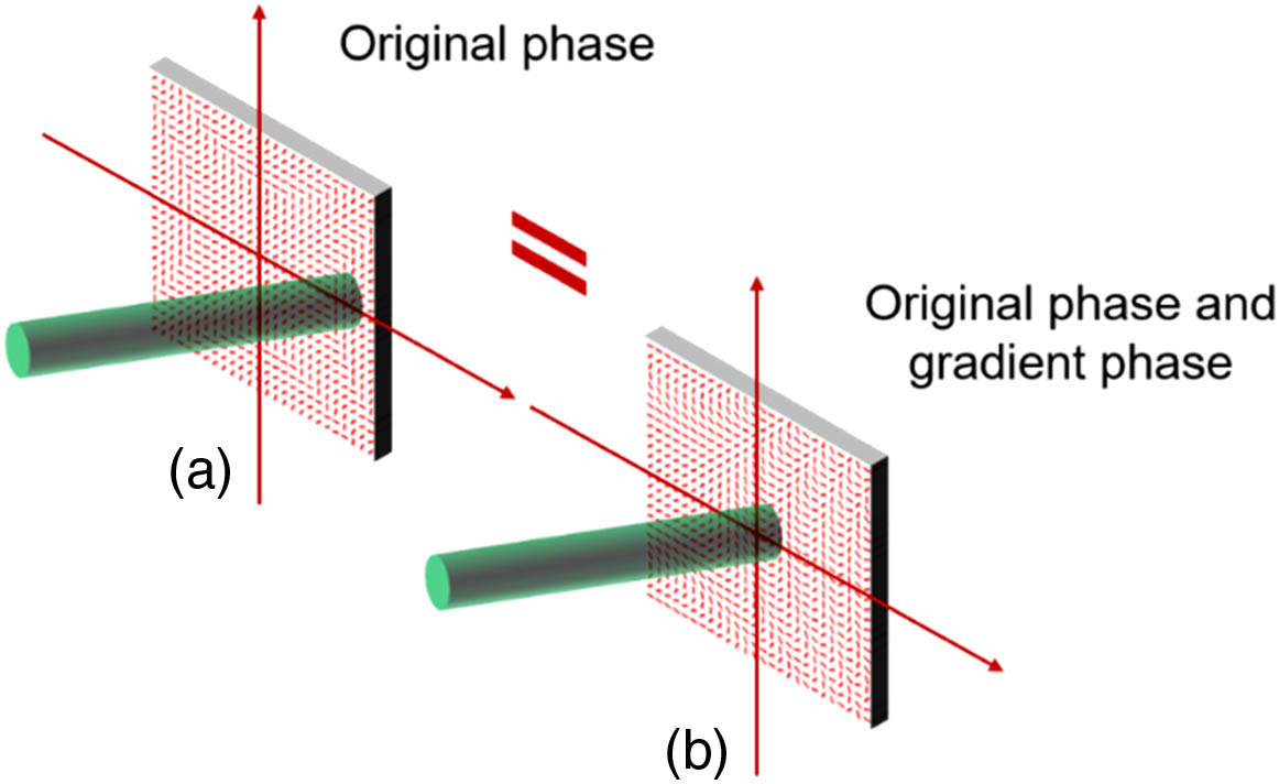
Photonic spin Hall effect (SHE) provides new opportunities for achieving spin-based photonics applications. However, flexibly manipulating the spin-dependent splitting (SDS) of photonic SHE and imposing extra phase modulation on the two spin components are always a challenge. Here, a controllable SHE mechanism based on phase function construction is reported. It is concluded that the phases with specific functional structures performing a coordinate translation are equivalent to integrating a gradient phase to the original phases. Hence, the original phase can be used for independent phase modulation, and the gradient phase originating from the coordinate translation is capable of manipulating the SDS. A metasurface with Pancharatnam–Berry phase that can impose conjugate phases to the two spin components of light is fabricated to verify this mechanism. By shifting the light position, the SDS is continuously manipulated in the visible region, which is successfully used for detecting the polarization ellipticity. The extra phase modulation is also performed with the original phase and thus enables measuring singular beams. It is anticipated that the controllable SHE manipulation method may open new avenues in the fields of spin photonics, optical sensing, optical communications, etc.
1 State Key Laboratory of Electronic Thin Films and Integrated Devices, School of Optoelectronic Science and Engineering, University of Electronic Science and Technology of China, Chengdu 610054, China
2 College of Electrical Engineering, Sichuan University, Chengdu 610065, China
3 e-mail: wangds@uestc.edu.cn
4 e-mail: hanz@scu.edu.cn
We report a watt-level passively -switched 2.8 μm mid-infrared multi-mode fiber laser by employing multi-layered two-dimensional MXene- as the saturable absorber (SA). The MXene- is fabricated by selectively etching aluminum layers in . The non-saturable loss, modulation depth, and saturable intensity of the SA at 2866 nm were measured to be 25.0%, 33.2%, and , respectively. The maximum average output power of the -switched fiber laser reached 1.09 W at 28.23% slope efficiency. The pulse repetition rate, shortest pulse width, pulse peak power, and single-pulse energy were 78.12 kHz, 1.04 μs, 13.4 W, and 13.93 μJ, respectively. This is the first demonstration of watt-level pulse generation in a mid-infrared fiber laser using low dimensional materials, to the best of our knowledge. These results indicate that the is a reliable and superior broadband SA for high power mid-infrared pulsed laser generation.
1 Wuhan National Laboratory for Optoelectronics and School of Optical and Electrical Information, Huazhong University of Science and Technology, Wuhan 430074, China
2 Department of Photonics Engineering, Technical University of Denmark, Building 343, 2800 Kgs. Lyngby, Denmark
The hybrid multiplexing technique reactivates optical interconnect as it offers multiple dimensions to dramatically enhance the data capacity of a single wavelength carrier. A straightforward method to realize hybrid multiplexing is to perform polarization multiplexing for mode-multiplexed signals, by utilizing a mode-transparent polarization beam splitter (MTPBS) which can process multiple modes simultaneously. However, present PBSs mainly work in the single-mode regime, and it is not easy to redesign the conventional PBS to accommodate multiple modes, due to the severe mode dispersion. Here, a novel MTPBS, which can tackle a group of modes simultaneously, is proposed and demonstrated. As a demonstration, the MTPBS supporting a total channel number of 13 is experimentally achieved, with low insertion loss and low modal/polarization cross talk. This work provides a new insight to realize hybrid multiplexing and represents a solution for high-density and large-capacity photonic integration.
1 School of Physics, State Key Laboratory for Mesoscopic Physics, Academy for Advanced Interdisciplinary Studies, and Nano-optoelectronics Frontier Center of Ministry of Education, Peking University, Beijing 100871, China
2 Key Laboratory of Photochemical Conversion and Optoelectronic Materials, Technical Institute of Physics and Chemistry, Chinese Academy of Sciences, Beijing 100190, China
3 State Key Laboratory of Precision Measurement Technology and Instruments, Department of Precision Instruments, Tsinghua University, Beijing 100084, China
4 Collaborative Innovation Center of Quantum Matter, Beijing, China
With the recent development of the metasurface, generating an optical vortex in optical far or near fields is realized in various ways. However, to generate vortices in both the near and far fields simultaneously is still a challenge, which has great potential in the future compact and versatile photonic system. Here, a bi-channel optical vortex generator in both the near and far fields is proposed and demonstrated within a single metasurface, where the surface plasmon vortex and the far-field optical vortex can be simultaneously generated under circularly polarized light. The ability of generating vortices with arbitrary topological charges is experimentally demonstrated, which agrees well with simulations. This approach provides great freedom to integrate different vortex generators in a single device, and offers new opportunities for integrated optical communications, trapping, and other related fields.
1 State Key Laboratory of Alternate Electrical Power System with Renewable Energy Sources, School of Renewable Energy, North China Electric Power University, Beijing 102206, China
2 School of Mathematics and Physics, North China Electric Power University, Beijing 102206, China
Single-nanowire solar cells with a unique light-concentration property are expected to exceed the Shockley–Queisser limit. The architecture of single nanowire is an important factor to regulate its optical performance. We designed a trilobal silicon nanowire (SiNW) with two equivalent scales that possesses superior light-absorption efficiency in the whole wavelength range and shows good tolerance for incident angle. The electric field distribution in this geometry is concentrated in the blade with small equivalent scale and pivot with large equivalent scale, respectively, in the short wavelength range and long wavelength range. Corresponding good light absorption of trilobal SiNW in the two wavelength ranges leads to stronger total light-absorption capacity than that of cylindrical SiNW. Trilobal single-nanowire solar cells can obtain a short-circuit current density () of , which provides a new choice for designing single nanowire with excellent light-capture capability.
1 Wuhan National Laboratory for Optoelectronics, School of Optical and Electronic Information, Huazhong University of Science and Technology, Wuhan 430074, China
2 College of Precision Instruments and Opto-electronics Engineering, Tianjin University, Tianjin 300072, China
BST photonic crystals were fabricated by magnetron sputtering and annealed at . By controlling the crystallinity and the oxygen vacancies of the ferroelectric photonic crystals, the optically and electrically controllable terahertz wave modulations were realized. The variation in refractive index of the 680°C annealed sample showed the highest modulation to the optical pump and increased to 11.9 due to the highest absorption near 532 nm. In the optical pump, the electrons from ions could be stimulated and captured by ions, and the ratio of observed increased with the increasing annealing temperature, indicating the increasing oxygen vacancies concentration, which increased the 532 nm optical absorption and contributed to the improved optical modulation. The excess Pb migrating to the surface at higher annealing temperature might be one reason for the degradation of optical modulation. The increasing polarization and leakage current could contribute to the increasing permittivity and loss with the increasing annealing temperature. Two different results were observed on the sample annealed at 680°C when the order of applying external optical and electric fields was changed, due to the different migration mechanisms of excited carriers. This work provides a potentially effective approach to fabricate THz sensing, imaging, and communications devices with multi-function in the modulation of optical and electric multi-fields.
1 LMAM, School of Mathematical Sciences, Peking University, Beijing 100871, China
2 State Key Laboratory of Membrane Biology, Beijing Key Laboratory of Cardiometabolic Molecular Medicine, Institute of Molecular Medicine, Peking University, Beijing 100871, China
3 Center for Bioinformatics, National Laboratory of Protein Engineering and Plant Genetic Engineering, School of Life Sciences, Peking University, Beijing 100871, China
4 School of Software and Microelectronics, Peking University, Beijing 100871, China
5 Beijing Advanced Innovation Center for Imaging Theory and Technology, Capital Normal University, Beijing 100871, China
6 e-mail: lychen@pku.edu.cn
7 e-mail: heng.mao@pku.edu.cn
Due to its ability of optical sectioning and low phototoxicity, -stacking light-sheet microscopy has been the tool of choice for in vivo imaging of the zebrafish brain. To image the zebrafish brain with a large field of view, the thickness of the Gaussian beam inevitably becomes several times greater than the system depth of field (DOF), where the fluorescence distributions outside the DOF will also be collected, blurring the image. In this paper, we propose a 3D deblurring method, aiming to redistribute the measured intensity of each pixel in a light-sheet image to in situ voxels by 3D deconvolution. By introducing a Hessian regularization term to maintain the continuity of the neuron distribution and using a modified stripe-removal algorithm, the reconstructed -stack images exhibit high contrast and a high signal-to-noise ratio. These performance characteristics can facilitate subsequent processing, such as 3D neuron registration, segmentation, and recognition.
1 Department of Engineering Physics, McMaster University, Hamilton, Ontario L8S 4L7, Canada
2 LioniX International BV, Enschede AL 7500, The Netherlands
This erratum corrects typos that appeared in Photon. Res.8, 127 (2020)PRHEIZ2327-912510.1364/PRJ.8.000127 in the text, a figure showing the experimental setup, and a table listing the absorption and emission cross section values used in simulations.
1 Instituto de Ciencias Nucleares, Universidad Nacional Autónoma de México, Apdo. Postal 70-543, Ciudad de México 04510, Mexico
2 Tecnologico de Monterrey, Escuela de Ingeniería y Ciencias, Ave. Eugenio Garza Sada 2501, Monterrey, N.L. 64849, Mexico
3 e-mail: dlopezmago@tec.mx
4 e-mail: alfred.uren@correo.nucleares.unam.mx
In this paper, we revisit the well-known Hong–Ou–Mandel (HOM) effect in which two photons, which meet at a beamsplitter, can interfere destructively, leading to null in coincidence counts. In a standard HOM measurement, the coincidence counts across the two output ports of the beamsplitter are monitored as the temporal delay between the two photons prior to the beamsplitter is varied, resulting in the well-known HOM dip. We show, both theoretically and experimentally, that by leaving the delay fixed at a particular value while relying on spectrally resolved coincidence photon counting, we can reconstruct the HOM dip, which would have been obtained through a standard delay-scanning, non-spectrally resolved HOM measurement. We show that our numerical reconstruction procedure exhibits a novel dispersion cancellation effect, to all orders. We discuss how our present work can lead to a drastic reduction in the time required to acquire a HOM interferogram, and specifically discuss how this could be of particular importance for the implementation of efficient quantum-optical coherence tomography devices.
1 State Key Laboratory of Crystal Materials, Shandong University, Jinan 250100, China
2 Key Laboratory of Laser & Infrared System, Ministry of Education, Shandong University, Qingdao 266237, China
3 Department of Electronics and Nanoengineering, Aalto University, Espoo FI-00076, Finland
4 e-mail: yhyanghe@gmail.com
Indium phosphide (InP) nanowires (NWs) have attracted significant attention due to their exotic properties that are different from the bulk counterparts, and have been widely used for light generation, amplification, detection, modulation, and switching, etc. Here, high-quality InP NWs were directly grown on a quartz substrate by the Au-nanoparticle assisted vapor-liquid-solid method. We thoroughly studied their nonlinear optical absorption properties at 1.06 μm by the open-aperture Z-scan method. Interestingly, a transition phenomenon from saturable absorption (SA) to reverse saturable absorption (RSA) was observed with the increase of the incident laser intensity. In the analysis, we found that the effective nonlinear absorption coefficient () under the SA process was 3 orders of magnitude larger than that during the RSA processes. Furthermore, the SA properties of InP NWs were experimentally verified by using them as a saturable absorber for a passively -switched solid-state laser at 1.06 μm, where the shortest pulse width of 462 ns and largest single pulse energy of 1.32 μJ were obtained. Moreover, the ultrafast carrier relaxation dynamics were basically studied, and the intra-band and inter-band ultrafast carrier relaxation times of 8.1 and 63.8 ps, respectively, were measured by a degenerate pump–probe method with the probe laser of 800 nm. These results well demonstrate the nonlinear optical absorption properties, which show the excellent light manipulating capabilities of InP NWs and pave a way for their applications in ultrafast nanophotonic devices.
1 Department of Physics, Changchun University of Science and Technology, Changchun 130022, China
2 e-mail: songxiaowei@cust.edu.cn
The comprehensive capture of near-field spatiotemporal information of surface plasmon polaritons (SPPs) is a prerequisite for revealing their physical nature. In this study, we first performed an independent, spatiotemporal imaging of the out-of-plane and in-plane components of SPP near-fields in a femtosecond light-excited trench using an obliquely incident time-resolved photoemission electron microscopy (TR-PEEM). We did the capture by imaging of the interference patterns induced by a superposition of the - or -polarized probe light, with the out-plane or in-plane components of SPP near-fields, under the noncollinear excitation mode. The method may be used to reconstruct a 3D SPP spatiotemporal field. Moreover, we demonstrated that the fringe shift of the interference patterns between the captured in-plane and out-of-plane components of the SPP field in PEEM images corresponds to the 1/4 fringe period, which is attributed to out of phase of the out-of-plane and in-plane near-field components of SPP. The resulting TR-PEEM images are supported by a classical wave mode and FDTD simulations. Essentially, the measured phase difference between the in-plane and out-of-plane components of the SPP indicated a rotating field component in the propagation plane, i.e., that the SPP exhibits an elliptically polarized electric field in the propagation plane. The experimental results presented herein provide direct evidence of SPP having the inherent attributes of transverse spin angular momentum.
Department of Printed Electronics Engineering, Sunchon National University Jeonnam 540-742, South Korea
The effect of tin-oxide (SnO) nanoparticles, which are obtained by indium-tin-oxide (ITO) treatment, on the p-GaN surface of GaN-based flip-chip blue micro-light-emitting diode (-LED) arrays is investigated. A thin Ag layer is deposited on the ITO-treated p-GaN surface by sputtering. SnO nanoparticles originate from inhomogeneous Schottky barrier heights (SBHs) at Ag/p-GaN contact. Therefore, effective SBH is reduced, which causes carrier transport into the -LED to enhance. 10 nm thick ITO-treated -LEDs show better optoelectronic characteristics among fabricated -LEDs owing to improved ohmic contact and highly reflective p-type reflectors. Basically, SnO nanoparticles help to make good ohmic contact, which results in improved carrier transport into -LEDs and thus results in increased optoelectronic performances.
1 Department of Electrical & Computer Engineering, University of California, San Diego, California 92093, USA
2 King Abdulaziz City for Science and Technology (KACST), Riyadh 11442, Saudi Arabia
We present an experimental demonstration of notch filters with arbitrary center wavelengths capable of tunable analog output power values varying between full extinction of 15 and 0 dB. Each filter is composed of highly modular apodized four-port Bragg add/drop filters to reduce the crosstalk between concatenated devices. The constructed photonic integrated circuit experimentally demonstrates spectra shaping using four independent notch filters. Each notch filter supports a bandwidth of and is shown to be suitable for realization of programmable photonic integrated circuits.


 Download:607次