

2020, 8(9) Column
Photonics Research 第8卷 第9期
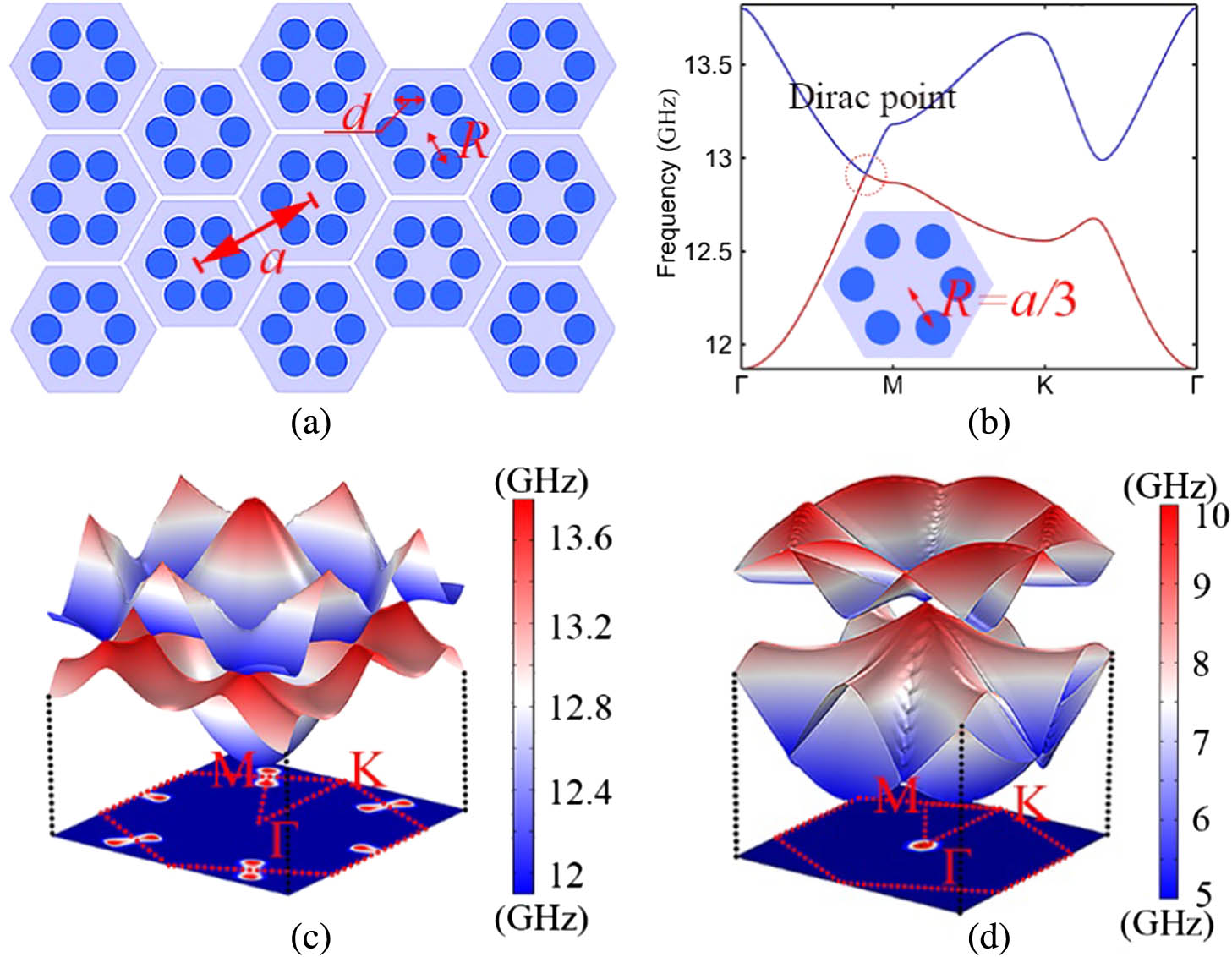
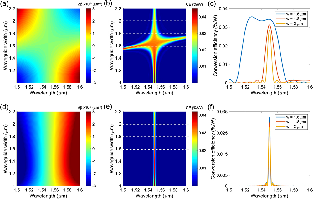
The recent realizations of a topological valley phase in a photonic crystal, an analog of gapped valleytronic materials in an electronic system, are limited to the valley Chern number of one. In this paper, we present a type of valley phase that can have a large valley Chern number of two or three. The valley phase transitions between the different valley Chern numbers (from one to three) are realized by changing the configuration of the unit cell. We demonstrate that these topological phases can guide the wave propagation robustly along a sharply bent domain wall. We believe our results are promising for the exploration of new topological phenomena in photonic systems.


Creating locally interacting Hamiltonians in the synthetic frequency dimension for photons Download:680次
Download:680次The recent emerging field of synthetic dimension in photonics offers a variety of opportunities for manipulating different internal degrees of freedom of photons such as the spectrum of light. While nonlinear optical effects can be incorporated into these photonic systems with synthetic dimensions, these nonlinear effects typically result in long-range interactions along the frequency axis. Thus, it has been difficult to use the synthetic dimension concept to study a large class of Hamiltonians that involves local interactions. Here we show that a Hamiltonian that is locally interacting along the synthetic dimension can be achieved in a dynamically modulated ring resonator incorporating

Influence of mixed organic cations on the nonlinear optical properties of lead tri-iodide perovskitesDownload:611次
Download:611次Metal halide perovskite materials have been widely studied recently due to their excellent optoelectronic properties. Among these materials, organic-inorganic hybrid perovskites have attracted much attention because of their relatively soft framework, which makes them more suitable for nonlinear optical (NLO) applications. However, there is rare physical mechanism study on the coexistence of two-photon absorption (TPA) and saturable absorption (SA) in organic-inorganic hybrid perovskite materials. To clarify this issue, the NLO properties of mixed cation perovskite
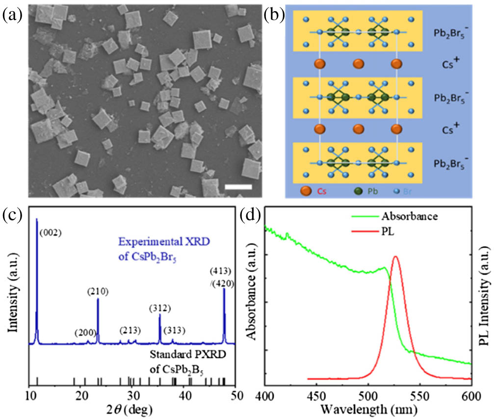
Mode selection and high-quality upconversion lasing from perovskite CsPb2Br5 microplatesDownload:626次
Download:626次In recent years, halide perovskite nanostructures have had great advances and have opened up a bright future for micro/nanolasers. However, upconversion lasing by two-photon excitation with mode selection and high quality factor in one device is still rarely reported. Herein, two lasing modes are demonstrated in the all-inorganic perovskite

Structural coloration techniques have improved display science due to their high durability in terms of resistance to bleaching and abrasion, and low energy consumption. Here, we propose and demonstrate an all-solid-state, large-area, lithography-free color filter that can switch structural color based on a doped semiconductor. Particularly, an indium-gallium-zinc-oxide (IGZO) thin film is used as a passive index-changing layer. The refractive index of the IGZO layer is tuned by controlling the charge carrier concentration; a hydrogen plasma treatment is used to control the conductivity of the IGZO layer. In this paper, we verify the color modulation using finite difference time domain simulations and experiments. The IGZO-based color filter technology proposed in this study will pave the way for charge-controlled tunable color filters displaying a wide gamut of colors on demand.

Linear and nonlinear photophysical properties of ZnSe/CdS/ZnS core/shell/shell type II nanocrystalsDownload:646次
Download:646次In this work, one kind of type II ZnSe/CdS/ZnS core/shell/shell nanocrystals (NCs) is synthesized, and their linear and nonlinear photophysical properties are investigated. Through measurements of the temperature-dependent photoluminescence spectra of NCs, their excitonic properties, including the coefficient of the bandgap change, coupling strength of the exciton acoustic phonons, exciton longitudinal optical (LO) phonons, and LO–phonon energy are revealed. Femtosecond transient absorption spectroscopy was employed to obtain insight into ultrafast processes occurring at the interface of ZnSe and CdS, such as those involving the injection of photo-induced electrons into the CdS shell, interfacial state bleaching, and charge separation time. At the end, their multiphoton absorption spectra were determined by using the z-scan technique, which yielded a maximum two-photon absorption cross section of 3717 GM at 820 nm and three-photon absorption cross section up to

Generation of squeezed states of light in arbitrary complex amplitude transverse distributionDownload:801次
Download:801次The squeezed state is important in quantum metrology and quantum information. The most effective generation tool known is the optical parametric oscillator (OPO). Currently, only the squeezed states of lower-order spatial modes can be generated by an OPO. However, the squeezed states of higher-order spatial modes are more useful for applications such as quantum metrology, quantum imaging, and quantum information. A major challenge for future applications is efficient generation. Here we use cascaded phase-only spatial light modulators to modulate the amplitude and phase of the incident fundamental mode squeezed state. This efficiently generates a series of squeezed higher-order Hermite–Gauss modes and a squeezed arbitrary complex amplitude distributed mode. The method may yield new applications in biophotonics, quantum metrology, and quantum information processing.
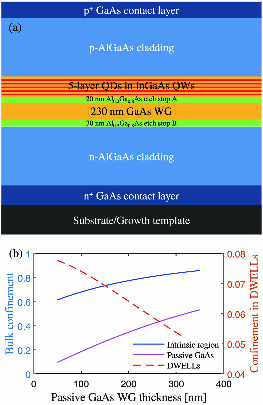
Quantum dot lasers are excellent on-chip light sources, offering high defect tolerance, low threshold, low temperature variation, and high feedback insensitivity. Yet a monolithic integration technique combining epitaxial quantum dot lasers with passive waveguides has not been demonstrated and is needed for complex photonic integrated circuits. We present here, for the first time to our knowledge, a monolithc offset quantum dot integration platform that permits formation of a laser cavity utilizing both the robust quantum dot active region and the versatility of passive GaAs waveguide structures. This platform is substrate agnostic and therefore compatible with the quantum dot lasers directly grown on Si. As an illustration of the potential of this platform, we designed and fabricated a 20 GHz mode-locked laser with a dispersion-engineered on-chip waveguide mirror. Due to the dispersion compensation effect of the waveguide mirror, the pulse width of the mode-locked laser is reduced by a factor of 2.8.

All-dielectric silicon metalens for two-dimensional particle manipulation in optical tweezersDownload:624次
Download:624次Dynamic control of compact chip-scale contactless manipulation of particles for bioscience applications remains a challenging endeavor, which is restrained by the balance between trapping efficiency and scalable apparatus. Metasurfaces offer the implementation of feasible optical tweezers on a planar platform for shaping the exerted optical force by a microscale-integrated device. Here we design and experimentally demonstrate a highly efficient silicon-based metalens for two-dimensional optical trapping in the near-infrared. Our metalens concept is based on the Pancharatnam–Berry phase, which enables the device for polarization-sensitive particle manipulation. Our optical trapping setup is capable of adjusting the position of both the metasurface lens and the particle chamber freely in three directions, which offers great freedom for optical trap adjustment and alignment. Two-dimensional (2D) particle manipulation is done with a relatively low-numerical-aperture metalens (

Synchronous nanoscale topographic and chemical mapping by differential-confocal controlled Raman microscopyDownload:626次
Download:626次Confocal Raman microscopy is currently used for label-free optical sensing and imaging within the biological, engineering, and physical sciences as well as in industry. However, currently these methods have limitations, including their low spatial resolution and poor focus stability, that restrict the breadth of new applications. This paper now introduces differential-confocal controlled Raman microscopy as a technique that fuses differential confocal microscopy and Raman spectroscopy, enabling the point-to-point collection of three-dimensional nanoscale topographic information with the simultaneous reconstruction of corresponding chemical information. The microscope collects the scattered Raman light together with the Rayleigh light, both as Rayleigh scattered and reflected light (these are normally filtered out in conventional confocal Raman systems). Inherent in the design of the instrument is a significant improvement in the axial focusing resolution of topographical features in the image (to
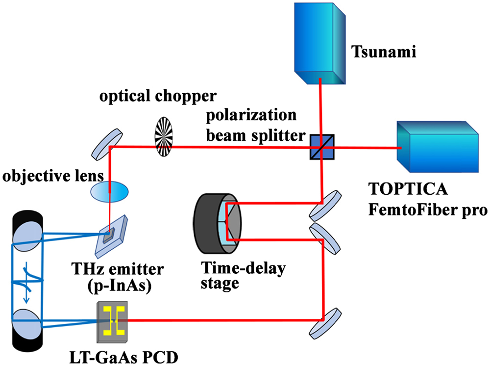
Low-temperature GaAs-based plasmonic photoconductive terahertz detector with Au nano-islandsDownload:660次
Download:660次We have fabricated low-temperature grown GaAs (LT-GaAs)-based plasmonic photoconductive antennas by RF sputtering of Au nanoparticles and have evaluated their terahertz detection properties. Localized surface plasmon resonance enhances the electric fields near the surface and increases the optical absorption of nanoparticles. The resonance frequency depends on the density of electrons, the effective electron mass, and the size and shape of the nanoparticles. Therefore, we tried to develop a high-sensitivity LT-GaAs photoconductive detector (PCD), which is effective over a wide range of wavelengths, by RF sputtering of Au nano-islands with a variety of aspect ratios from 1.2 to 5.1 on the dipole gap region of the PCD. As a result, we succeeded in increasing the sensitivity by 29% and 40% in the amplitude of observed terahertz pulse for 800 nm and 1560 nm femtosecond laser excitations, respectively.

Exceptional points are spectral singularities in open quantum and wave systems that exhibit a strong spectral response to perturbations. This feature can be exploited for a new generation of sensors. This paper explains the basic mechanism and comprehensively reviews the recent developments. In particular, it highlights the influence of classical noise and fundamental limitations due to quantum noise.

Weak measurement has been shown to play important roles in the investigation of both fundamental and practical problems. Anomalous weak values are generally believed to be observed only when post-selection is performed, i.e., only a particular subset of the data is considered. Here, we experimentally demonstrate that an anomalous weak value can be obtained without discarding any data by performing a sequential weak measurement on a single-qubit system. By controlling the blazing density of the hologram on a spatial light modulator, the measurement strength can be conveniently controlled. Such an anomalous phenomenon disappears when the measurement strength of the first observable becomes strong. Moreover, we find that the anomalous weak value cannot be observed without post-selection when the sequential measurement is performed on each of the components of a two-qubit system, which confirms that the observed anomalous weak value is based on sequential weak measurement of two noncommutative operators.
Broadband quasi-phase-matching in dispersion-engineered all-optically poled silicon nitride waveguidesDownload:640次
Download:640次Quasi-phase-matching (QPM) has become one of the most common approaches for increasing the efficiency of nonlinear three-wave mixing processes in integrated photonic circuits. Here, we provide a study of dispersion engineering of QPM second-harmonic (SH) generation in stoichiometric silicon nitride (

In this work, on-chip chalcogenide glass photonic integrations with several fundamental photonic building blocks are designed and fabricated based on the
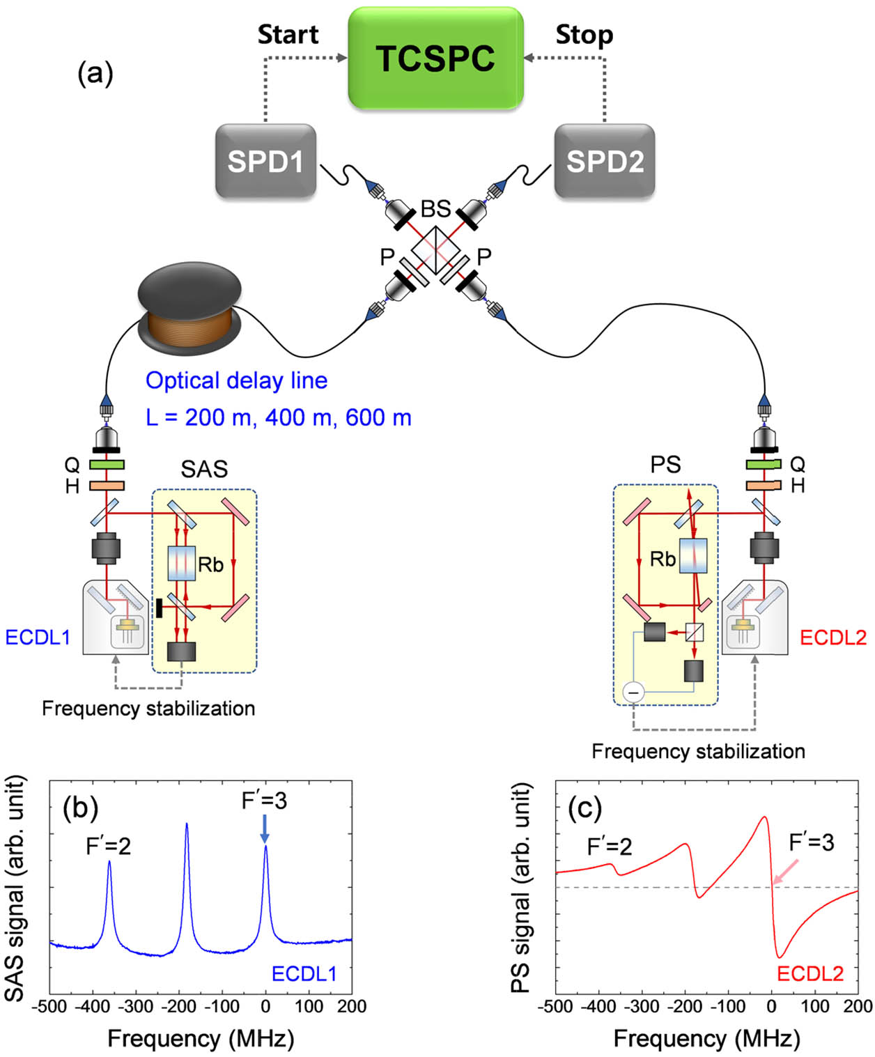
Interference between two completely independent photons lies at the heart of many photonic quantum information applications such as quantum repeaters, teleportation, and quantum key distribution. Here, we report the observation of Hong–Ou–Mandel (HOM) interference with two independent continuous-wave coherent light sources that are neither synchronized nor share any common reference. To prepare indistinguishable photons from two independent laser sources, we employ high-precision frequency-stabilization techniques using the

Self-powered electronic paper with energy supplies and information inputs solely from mechanical motionsDownload:633次
Download:633次The electronic paper (E-paper) displays features such as flexibility, sunlight visibility, and low power consumption, which makes it ideal for Internet of Things (IoT) applications where the goal is to eliminate bulky power modules. Here, we report a unique self-powered E-paper (SPEP), where information inputs and energy supplies are all converted from mechanical motion by a triboelectric nanogenerator (TENG). The operation of an electrophoretic E-paper is first investigated, identifying the current density as a determinative parameter for driving pigment particle motion and color change. Electrical and optical responses of the E-paper driven by a sliding-mode TENG are then found to be consistent with that under a current source mode. All-in-one monochromic and chromatic SPEPs integrated with a flexible transparent TENG are finally demonstrated, and a pixelated SPEP is discussed for future research. The sliding-driven mechanism of SPEP allows for a potential handwriting function, is free of an extra power supply, and promises undoubtedly a wide range of future applications.

Cascaded multilayer nano-kirigami for extensible 3D nanofabrication and visible light manipulationDownload:677次
Download:677次Nano-kirigami enables direct and versatile shape transformations from two-dimensional predesigns to three-dimensional (3D) architectures in microscale/nanoscale. Here a new and extensible strategy for cascaded multilayer nano-kirigami is demonstrated in a gold/silicon nitride (Au/SiN) bilayer nanofilm for 3D nanofabrication and visible light manipulation. By employing a focused ion-beam-based Boolean irradiation, rich 3D shape transformation and nested multilayer nanostructures are precisely manufactured, which are well reproduced by developing a modified mechanical model. Based on the multilayer and deformable features of the nano-kirigami structures, potentials in manipulating the phase and intensity of visible light are explored. The developed new nano-kirigami strategies, as well as the novel exotic 3D nanostructures, could be helpful to build a novel platform for 3D nanofabrication and find potential applications in microelectromechanical/nanoelectromechanical systems, holographic display, plasmonics, nanophotonics, biophotonics, etc.
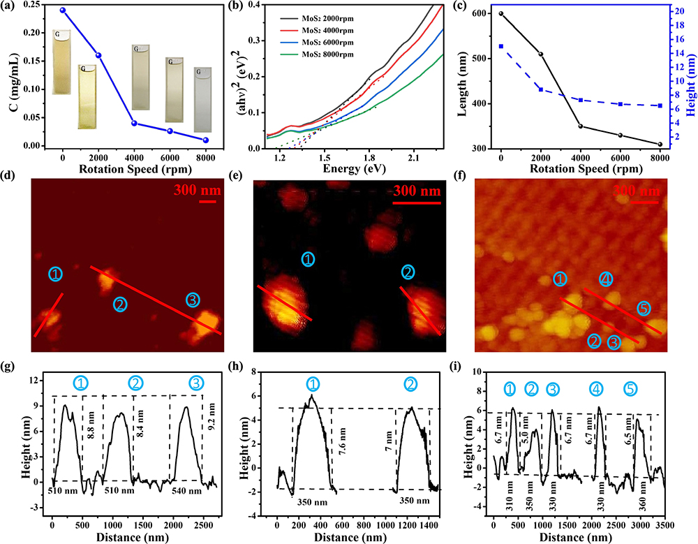
Saturable and reverse saturable absorption in molybdenum disulfide dispersion and film by defect engineeringDownload:771次
Download:771次Understanding and controlling defect in two-dimensional materials is important for both linear and nonlinear optoelectronic devices, especially in terms of tuning nonlinear optical absorption. Taking advantage of an atomic defect formed easily by smaller size, molybdenum disulfide nanosheet is prepared successfully with a different size by gradient centrifugation. Interestingly, size-dependent sulfur vacancies are observed by high-resolution X-ray photoelectron spectroscopy, atomic force microscopy, and transmission electron microscopy. The defect effect on nonlinear absorption is investigated by Z-scan measurement at the wavelength of 800 nm. The results suggest the transition from saturable absorption to reverse saturable absorption can be observed in both dispersions and films. First principle calculations suggest that sulfur vacancies act as the trap state to capture the excited electrons. Moreover, an energy-level model with the trap state is put forward to explain the role of the sulfur vacancy defect in nonlinear optical absorption. The results suggest that saturable absorption and reverse saturable absorption originate from the competition between the excited, defect state and ground state absorption. Our finding provides a way to tune the nonlinear optical performance of optoelectronic devices by defect engineering.

We report an experimental implementation of free-space quantum secure direct communication based on single photons. The quantum communication scheme uses phase encoding, and the asymmetric Mach–Zehnder interferometer is optimized so as to automatically compensate phase drift of the photons during their transitions over the free-space medium. At a 16 MHz pulse repetition frequency, an information transmission rate of 500 bps over a 10 m free space with a mean quantum bit error rate of

Single-photon light detection and ranging (lidar) offers single-photon sensitivity and picosecond timing resolution, which is desirable for high-precision three-dimensional (3D) imaging over long distances. Despite important progress, further extending the imaging range presents enormous challenges because only a few echo photons return and are mixed with strong noise. Here, we tackled these challenges by constructing a high-efficiency, low-noise coaxial single-photon lidar system and developing a long-range-tailored computational algorithm that provides high photon efficiency and good noise tolerance. Using this technique, we experimentally demonstrated active single-photon 3D imaging at a distance of up to 45 km in an urban environment, with a low return-signal level of

Towards the integration of nanoemitters by direct laser writing on optical glass waveguidesDownload:523次
Download:523次A major challenge towards nanophotonics is the integration of nanoemitters on optical chips. Combining the optical properties of nanoemitters with the benefits of integration and scalability of integrated optics is still a major issue to overcome. In this work, we demonstrate the integration of nanoemitters positioned in a controlled manner onto a substrate and onto an optical ion-exchanged glass waveguide via direct laser writing based on two-photon polymerization. Our nanoemitters are colloidal CdSe/ZnS quantum dots (QDs) embedded in polymeric nanostructures. By varying the laser parameters during the patterning process, we make size-controlled QD-polymer nanostructures that were systematically characterized using optical and structural methods. Structures as small as 17 nm in height were fabricated. The well-controlled QD-polymer nanostructure systems were then successfully integrated onto a new photonic platform for nanophotonics made of an ion-exchanged waveguide. We show that our QDs maintain their light emitting quality after integration as verified by photoluminescence (PL) measurements. Ultimately, QD emission coupled to our waveguides is detected through a home-built fiber-edge coupling PL measurement setup. Our results show the potential for future integration of nanoemitters onto complex photonic chips.

影响因子:7.6
CN:31-2126/O4
ISSN:2327-9125


公告
动态信息
动态信息 丨 2024-04-11
PR Highlight (Vol. 11, Iss. 12): 亮点 | 十亿像素级、高通量的无透镜偏振编码叠层成像技术动态信息 丨 2024-03-29
PR 封面故事 (Vol. 12, Iss. 3): 封面 | 基于时空编码神经网络的像差感知超分辨成像动态信息 丨 2024-03-25
PR 封面故事 (Vol. 12, Iss. 1) 光涡旋与手性器件微纳3D打印动态信息 丨 2024-03-14
PR Highlight (Vol. 12, Iss. 1): 同步双脉冲激光烧蚀中的气泡相互作用效应动态信息 丨 2024-03-04
PR Highlight (Vol. 11, Iss. 12): 利用钙钛矿微米线异质结构,实现高性能偏振敏感光电探测激光评论微信公众号

点击菜单“联系编辑”即可添加期刊编辑为好友啦