1 浙江大学极端光学技术与仪器全国重点实验室,浙江 杭州 310027
2 之江实验室,浙江 杭州 311121
双光子直写技术凭借其高精度、任意三维结构刻写、高成本效益、材料设计高自由度等特点,已被成功应用到多种微纳光学器件的刻写中。基于双光子直写的微纳光学器件应用不断拓展,对刻写分辨率和通量都提出了更高的需求。超分辨激光纳米直写和高通量激光直写技术使得双光子直写具有nm级精度与cm级尺寸的跨尺度加工能力,进一步拓展了基于双光子直写的微纳光学器件研究领域。本文首先对双光子直写原理进行概述,介绍本课题组在利用双光子直写技术制造衍射光学器件、光纤集成器件方面的研究进展;然后,介绍本课题组在使用超分辨激光直写技术制备纳米光子器件方面的拓展研究,并展示了高精度、高通量激光直写技术在大面积刻写微纳光学器件上的技术优势。
激光直写 双光子直写 微纳光学器件 纳米光刻 高通量刻写 光学学报
2023, 43(16): 1623013
1 之江实验室智能芯片与器件研究中心,浙江 杭州 311121
2 浙江大学光电科学与工程学院极端光学技术与仪器全国重点实验室,浙江 杭州 310027
3 上海电力大学电子与信息工程学院,上海 200090
4 浙江大学杭州国际科创中心, 浙江 杭州 311200
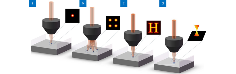
Overview: Two-photon lithography (TPL) has been a research hotspot in 3D micro/nano writing technology due to its characteristics of high resolution, low thermal influence, a wide range of processed materials, low environmental requirements, and 3D processing capability. It has shown unique advantages in the fields of life science, material engineering, micro/nano optics, microfluidic, micro machinery, and so on. This paper summarizes the research works done by researchers on different writing methods to improve TPL processing efficiency. Single-beam writing is the main method for TPL, which mainly depends on the speed of the scanning device. Single-beam writing has the advantages of simple system and high-quality beam, and it is easy to combine various effects to improve writing results. It mainly includes scanning modes based on the translation stage, galvo, polygon laser scanner, and acousto-optic deflector (AOD) (Fig. 2). All these modes have advantages and disadvantages. As for the scanning speed comparison, polygon laser scanner and AOD have relatively faster writing rates (faster than m/s). Multi-foci parallel lithography can obviously promote efficiency, elevating the speed by dozens or even hundreds of thousands of times, mainly based on spatial light modulator (SLM), digital micromirror device (DMD), microlens array (MLA), diffractive optical elements (DOE), multi-beam interference, and so on (Figs. 3-15). Multi-foci parallel lithography based on SLM is most widely used owing to its high efficiency and ability to flexible and independent control of each single beam, but the refresh rate is still insufficient. DMD has a higher refreshing rate (32 kHz), but the state-of-the-art beam parallelism realized by DMD is severely limited. More parallel beams are further required for improving the processing efficiency. The 2D pattern exposure method based on SLM or DMD can further improve the TPL efficiency with the superiority of generating flexibly designed pattern (Figs. 16-18). However, the 2D projection exposure technology is still difficult to achieve high writing precision, especially the axial resolution. An available method to improve the axial precision is spatially and temporally focusing an ultrafast laser to implement a strong intensity gradient at the spatial focal plane that restricts polymerization within a thin layer. The 3D projection method will be the most efficient writing method in the future, especially in 3D device processing (Figs. 19-20). Researchers used this technique to make hollow tubular and conical helices structures, increasing the processing speed by 600 times. However, the research results show that the current 3D projection can only process simple 3D structures. Further researches on 3D exposure processing of complex structures are expected, which will effectively expand its application in various fields. Authors believe that with the effort of researchers on efficiency improvement gradually, TPL can further highlight its advantages to promote the development of life science, materials engineering, micro-nano optics, and many other fields.
飞秒激光直写 双光子光刻 单光束扫描 多焦点并行 面曝光 体曝光 femtosecond laser direct writing two-photon lithography single-beam scanning multi-focus parallelism pattern projection 3D projection exposure 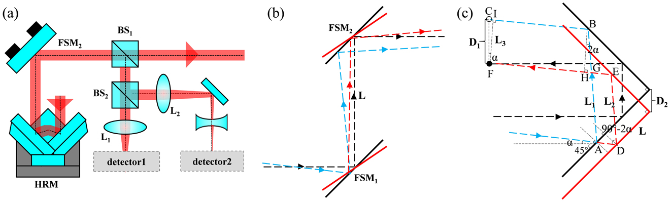
Author Affiliations
Abstract
1 Research Center for Intelligent Chips and Devices, Zhejiang Lab, Hangzhou 311121, China
2 State Key Laboratory of Modern Optical Instrumentation, Department of Optical Engineering, Zhejiang University, Hangzhou 310027, China
3 College of Electronics and Information Engineering, Shanghai University of Electric Power, Shanghai 200090, China
We propose a new method for the development of multi-beam systems for the spatial alignment and stability of beams based on the error separation technique. This method avoids alignment errors caused by coupling effect of piezoelectric devices, inaccurate correction calculations, and detection mode of the angular deviation. According to the results by external detectors, the error value of spatial alignment and the root mean square (RMS) of deviations under control during 1 h can be equivalent to approximately 0.87 and 1.06 nm at the sample plane under an oil immersion lens (focal length f). The RMS of deviations is less than one-third of those currently reported for multi-beam systems; therefore, higher alignment and stability accuracy can be achieved with our proposed method.
Chinese Optics Letters
2023, 21(3): 031201
浙江大学 光电科学与工程学院, 浙江 杭州 310058
为了拓展荧光辐射差分(Fluorescence Emission Difference,FED)显微术的应用, 使得该方法可以同时对生物样品的不同组织结构进行超分辨成像, 本文对双色FED显微系统展开了研究。FED的基本原理是将实心光斑扫描得到的共焦显微图像减去空心光斑扫描得到的负共焦图像, 以此获得超分辨显微图像。在对单色FED显微系统进行研究后, 本文提出了一种可行的双色FED显微成像系统方案。实验结果表明, 在488 nm和640 nm激发光下, 该系统在荧光颗粒上分别实现了135 nm和160 nm的空间分辨率, 另外也能对生物样品的不同组织进行多色同时超分辨显微成像, 满足了实际应用的要求。
光学显微 衍射极限 荧光 荧光辐射差分 超分辨 optical microscopy diffraction limit fluorescence fluorescence emission difference(FED) super-resolution
利用电荷耦合器件(CCD)在一定范围内与光照度成线性响应的特性,提出了一种通过双帧图像融合的方法,进行脉冲激光束散角的检测,并通过Matlab数学仿真和实验验证了其可行性和准确性。该方法扩大了光照度适用范围;弥补了CCD动态响应范围不宽的缺陷,很好的解决了脉冲激光束散角测量精度不高的问题。实验结果显示,该方法的测量精度为2%。
测量 脉冲激光 束散角 图像融合 双帧图像


