
Author Affiliations
Abstract
1 State Key Laboratory of Superlattices and Microstructures, Institute of Semiconductors, Chinese Academy of Sciences, Beijing 100083, China
2 Center of Materials Science and Optoelectronics Engineering, University of Chinese Academy of Sciences, Beijing 100190, China
(Ga,Fe)Sb is a promising magnetic semiconductor (MS) for spintronic applications because its Curie temperature (TC) is above 300 K when the Fe concentration is higher than 20%. However, the anisotropy constant Ku of (Ga,Fe)Sb is below 7.6 × 10³ erg/cm3 when Fe concentration is lower than 30%, which is one order of magnitude lower than that of (Ga,Mn)As. To address this issue, we grew Ga1-x-yFexNiySb films with almost the same x (≈24%) and different y to characterize their magnetic and electrical transport properties. We found that the magnetic anisotropy of Ga0.76-yFe0.24NiySb can be enhanced by increasing y, in which Ku is negligible at y = 1.7% but increases to 3.8 × 10⁵ erg/cm3 at y = 6.1% (TC = 354 K). In addition, the hole mobility (μ) of Ga1-x-yFexNiySb reaches 31.3 cm2/(V?s) at x = 23.7%, y = 1.7% (TC = 319 K), which is much higher than the mobility of Ga1-xFexSb at x = 25.2% (μ = 6.2 cm2/(V?s)). Our results provide useful information for enhancing the magnetic anisotropy and hole mobility of (Ga,Fe)Sb by using Ni co-doping.
magnetic semiconductor molecular beam epitaxy Fe-Ni co-doping magnetic anisotropy hole mobility Journal of Semiconductors
2024, 45(1): 012101
1 亚稳材料制备技术与科学国家重点实验室,燕山大学材料科学与工程学院,河北 秦皇岛 066004
2 威海中玻新材料技术研发有限公司,山东 威海264200
3 唐山学院,河北 唐山 063000
构建宽窄带隙同型异质结构的双层薄膜是提高透明导电薄膜光电性能的新思路。采用基于密度泛函的第一性原理,对本征和掺杂SnO2/SnSe2的电子结构、光学性质、载流子迁移率、电荷分布、能带排列进行计算。结果表明:本征和掺杂SnO2/SnSe2电子结构内部存在的电势差会使体系内部的电子向着界面处或SnSe2处转移,处于界面处的电子会在界面间隙内形成二维电子气并在界面处高速移动,从而提高了载流子的迁移率,而处于SnSe2处的电子由于没有杂质离子散射的影响迁移率也相应提高,4种不同掺杂类型异质结构的载流子迁移率分别为772.82、5 286.04、2 656.90 m2/(S·V)和17 724.60 m2/(S·V),光学透过率在80%以上。
透明导电薄膜 异质结构 第一性原理 载流子迁移率 transparent conductive oxide thin films heterostructures first principles carrier mobility
1 北京理工大学光电学院,北京 100081
2 北京理工大学长三角研究院,浙江 嘉兴 314019
采用混相配体交换的方法成功实现了载流子迁移率近2个量级的提升,达到1 cm2/(V·s),同时还可以灵活调控N型、本征型和P型等掺杂类型。在此基础上,使用本征型碲化汞胶体量子点薄膜制备短波及中波红外光伏型探测器。截止波长为1.9 μm的短波红外探测器在300 K下的响应率为0.9 A/W,比探测率为4×1011 Jones;截止波长为4.2 μm的中波红外探测器在110 K下的响应率为1.1 A/W,比探测率为1.2×1011 Jones。在没有施加偏置电压的情况下,300 K下的短波红外光电探测器的外量子效率可以达到61%,110 K下的中波红外光电探测器的外量子效率可以达到30%。
探测器 量子点 高迁移率 光伏型红外光电探测器 配体交换 光学学报
2023, 43(22): 2204002
1 中建材(洛阳)新能源有限公司,洛阳 471000
2 河南理工大学材料科学与工程学院,焦作 454000
基于密度泛函理论研究了Au、Cu、Sb掺杂CdTe体系的电子结构和光学性能。Au、Cu、Sb掺杂CdTe体系均能稳定存在,过渡金属原子与Cd原子轨道的杂化减小了CdTe的带隙,提高了CdTe对可见光的利用,同时降低了光生电子从价带跃迁到导带所需的能量,从而促进了更多的光生电子发生迁移,大大提高了其光学性能。三种掺杂体系中Sb/CdTe体系在可见光范围内光吸收系数提升最显著,其光生电子和光生空穴迁移率相对于CdTe体系分别增加5.97倍和15.54倍。通过计算掺杂体系的能带、态密度、电子布居、光吸收函数、载流子迁移率,从理论上揭示了Au、Cu、Sb提高CdTe光学性能的机理。
第一性原理 电子性质 光学性能 载流子迁移 CdTe CdTe first-principle electronic property optical property carrier mobility

Author Affiliations
Abstract
1 College of Electronic and Information Engineering, Shenzhen University, Shenzhen 518060, China
2 Institute of Microscale Optoelectronics (IMO), Shenzhen University, Shenzhen 518060, China
3 State Key Laboratory of Advanced Displays and Optoelectronics Technologies, The Hong Kong University of Science and Technology, Clear Water Bay, Kowloon, Hong Kong, China
Indium-tin-zinc oxide (ITZO) thin-film transistor (TFT) technology holds promise for achieving high mobility and offers significant opportunities for commercialization. This paper provides a review of progress made in improving the mobility of ITZO TFTs. This paper begins by describing the development and current status of metal-oxide TFTs, and then goes on to explain the advantages of selecting ITZO as the TFT channel layer. The evaluation criteria for TFTs are subsequently introduced, and the reasons and significance of enhancing mobility are clarified. This paper then explores the development of high-mobility ITZO TFTs from five perspectives: active layer optimization, gate dielectric optimization, electrode optimization, interface optimization, and device structure optimization. Finally, a summary and outlook of the research field are presented.
thin-film transistor (TFT) indium-tin-zinc oxide (ITZO) TFT mobility active matrix (AM) displays Journal of Semiconductors
2023, 44(9): 091602
Author Affiliations
Abstract
1 School of Microelectronics, University of Science and Technology of China, Hefei 230026, China
2 Dynax Semiconductor Inc., Suzhou 215300, China
3 Department of Micro- and Nanoelectronics, Saint Petersburg Electrotechnical University, Saint Petersburg 197376, Russia
A physics-based analytical expression that predicts the charge, electrical field and potential distributions along the gated region of the GaN HEMT channel has been developed. Unlike the gradual channel approximation (GCA), the proposed model considers the non-uniform variation of the concentration under the gated region as a function of terminal applied voltages. In addition, the model can capture the influence of mobility and channel temperature on the charge distribution trend. The comparison with the hydrodynamic (HD) numerical simulation showed a high agreement of the proposed model with numerical data for different bias conditions considering the self-heating and quantization of the electron concentration. The analytical nature of the model allows us to reduce the computational and time cost of the simulation. Also, it can be used as a core expression to develop a complete physics-based transistor Ⅳ model without GCA limitation.
AlGaN/GaN (HEMTs) 2DEG charge distribution electron mobility hydrodynamic model channel temperature Journal of Semiconductors
2023, 44(8): 082802
Author Affiliations
Abstract
1 State Key Laboratory of Electronic Thin Films and Integrated Devices, University of Electronic Science and Technology of China, Chengdu 610054, China
2 Key Laboratory of Nanodevices and Applications, Suzhou Institute of Nano-tech and Nano-bionics, CAS, Suzhou 215123, China
3 Institute of Electronic and Information Engineering, University of Electronic Science and Technology of China, Dongguan 523808, China
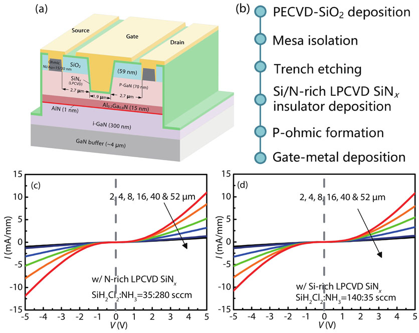
In this work, the GaN p-MISFET with LPCVD-SiNx is studied as a gate dielectric to improve device performance. By changing the Si/N stoichiometry of SiNx, it is found that the channel hole mobility can be effectively enhanced with Si-rich SiNx gate dielectric, which leads to a respectably improved drive current of GaN p-FET. The record high channel mobility of 19.4 cm2/(V?s) was achieved in the device featuring an Enhancement-mode channel. Benefiting from the significantly improved channel mobility, the fabricated E-mode GaN p-MISFET is capable of delivering a decent-high current of 1.6 mA/mm, while simultaneously featuring a negative threshold-voltage (VTH) of –2.3 V (defining at a stringent criteria of 10 μA/mm). The device also exhibits a well pinch-off at 0 V with low leakage current of 1 nA/mm. This suggests that a decent E-mode operation of the fabricated p-FET is obtained. In addition, the VTH shows excellent stability, while the threshold-voltage hysteresis ΔVTH is as small as 0.1 V for a gate voltage swing up to –10 V, which is among the best results reported in the literature. The results indicate that optimizing the Si/N stoichiometry of LPCVD-SiNx is a promising approach to improve the device performance of GaN p-MISFET.
p-channel GaN p-FET LPCVD channel mobility hole mobility enhancement-mode Journal of Semiconductors
2023, 44(8): 082801
采用综合考虑温度、电场强度、载流子浓度的普遍迁移率模型, 利用实际太阳能光谱和非富勒烯材料的吸收系数来计算载流子的产生, 结合漂移扩散方程、电流连续性方程等对高效率有机太阳电池进行理论建模。利用该模型计算了器件的电流-电压曲线、开路电压-光照强度曲线和短路电流-光照强度曲线。结果发现, 利用该模型计算的电流-电压曲线与实验数据符合很好, 其他两种曲线也与实验数据符合较好。此外, 利用该模型分析了能量无序度对器件性能的影响, 结果表明减小材料的能量无序度可以提高有机太阳电池的性能。
迁移率 非富勒烯 有机太阳电池 理论建模 能量无序度 mobility non-fullerene organic solar cells theoretical modeling energy disorder


