


期刊基本信息
创刊:
1974年 • 月刊
名称:
光电工程
英文:
Opto-Electronic Engineering
主管单位:
中国科学院
主办单位:
中国科学院光电技术研究所;中国光学学会
出版单位:
光电工程编辑部
主编:
罗先刚
ISSN:
1003-501X
刊号:
CN 51-1346/O4
电话:
028-85100579
邮箱:
地址:
四川省成都市双流350信箱《光电工程》编辑部
邮编:
610209
定价:
90元/期

光电工程 第50卷 第3期
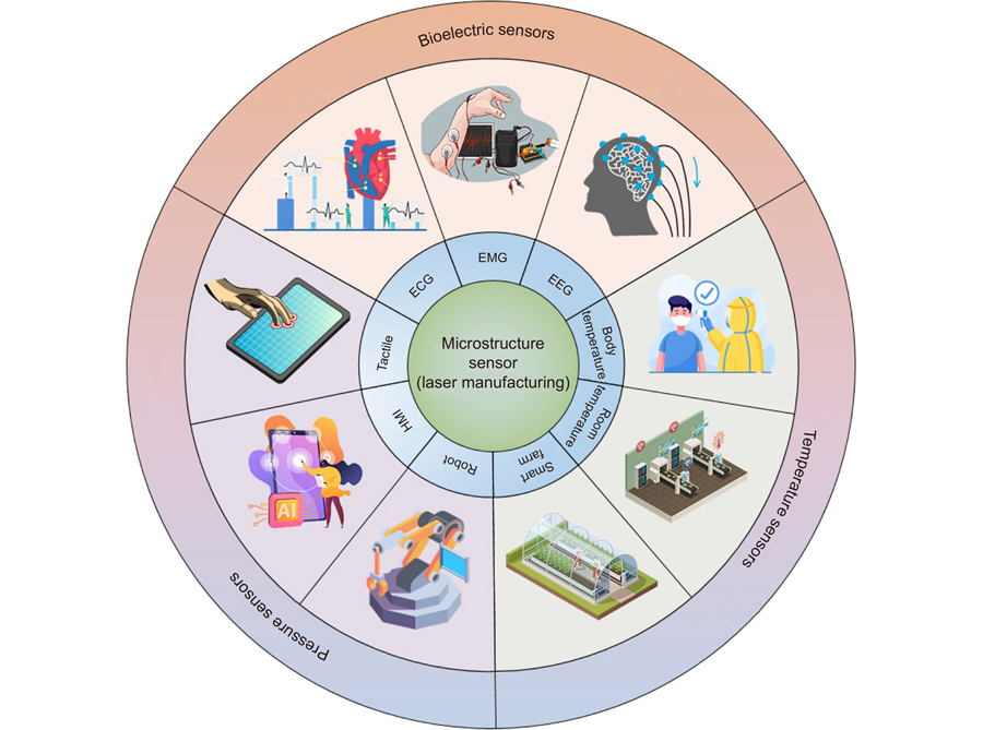
Overview: Microstructure sensor is a kind of sensor with a 2D or 3D micron-scale structure prepared by advanced manufacturing technology. It is used as a sensitive part to enhance the transmission characteristics of physical, chemical, and biological signals to the environment, and convert the external signals into electrical signals. The microstructure is generally a regular or disordered structure, usually in the shape of microspheres, microcolumns, microcones, microgrooves and micropores. The microstructures with different shapes can realize the functions of puncture, pressure transmission, vibration transmission, drug transmission, bioelectric transmission, heat transmission, sound transmission, gas adsorption, and so on. In recent years, researchers from all over the world have gradually attached great importance to the research on the manufacturing technology of microstructure sensors. At present, researchers have proposed the MEMS manufacturing processes, such as reactive ion etching and chemical vapor deposition, to achieve mass manufacturing of high-precision microstructures on flexible polymer materials and rigid materials. In addition, some researchers have also proposed the manufacturing processes such as template method, self-assembly, nanoimprinting, and soft lithography to realize microstructure manufacturing. However, the above-mentioned manufacturing processes usually cannot prepare microstructure in one step, which has the problems of complex process, high production cost, limited processing materials, and unable to control the microstructure morphology. In contrast, laser manufacturing technology has the advantages of non-contact processing, no mask, customizable manufacturing, etc. By optimizing the parameters of laser process (such as laser power, scanning speed, filling mode and scanning path), it can achieve efficient and low-cost manufacturing of microstructures with different sizes and shapes. Therefore, using laser manufacturing technology to realize microstructure manufacturing and applying it to bioelectricity, temperature, and pressure sensors has become a research hotspot in microstructure sensor manufacturing technology. Laser manufacturing technology mainly includes laser ablation, laser direct writing, laser induction, laser-template processing, etc. Laser ablation is an auxiliary heating process based on the thermochemical and thermophysical effects of a laser beam, which melts the materials to be processed to realize structural forming. Laser direct writing is a manufacturing process that focuses high-energy photon beams on the materials to be processed to produce a photochemical process, and manufacturing the structures through material removal. Laser-induced modification is a manufacturing process to change the physical and chemical properties of the materials to be processed. Laser-template processing is a manufacturing process that uses a laser to produce microstructure molds on silicon, glass, polymer, and other substrates, and then uses soft lithography technology to reverse die the structures on the molds. Based on the interaction between the laser and materials, the induction, removal, and migration of materials to be processed can be realized. By adjusting the laser processing mode and processing parameters, the controlled manufacturing of the 2D or 3D microstructures or the controlled preparation of functional materials for the sensitive units can be realized, breaking through the limitations of efficiency and cost of traditional manufacturing methods for microstructures. In this paper, the types, functions, and manufacturing technologies of microstructures are summarized and classified. The preparation processes of laser manufacturing technology and other advanced manufacturing technologies of microstructures are summarized. The applications of microstructure sensors prepared by laser ablation, laser direct writing, laser induction, and laser-template processing technology in bioelectric sensing, temperature sensing, and pressure sensing are described in detail. Finally, the development trend of the laser manufacturing technology for microstructure sensors is summarized and prospected.
激光制造 微结构 生物电传感器 温度传感器 压力传感器 laser manufacturing microstructure bioelectric sensors temperature sensors pressure sensors 

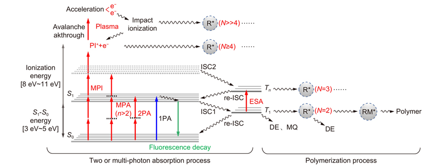

Overview: Femtosecond laser two-photon polymerization (TPP) micro-nanofabrication technology is a new type of three-dimensional lithography technology that integrates nonlinear optics, ultra-fast pulsed laser, microscopic imaging, ultra-high-precision positioning, three-dimensional (3D) graphics CAD modeling, and photochemical materials. It has the characteristics of simplicity, low cost, high resolution, true 3D, and so on. Different from the technical route of shortening the wavelength of the traditional lithography, this TPP technology breaks through the optical diffraction limit using the ultrafast laser in the near-infrared and the nonlinear optical effect of the interaction between the laser and the material. TPP can achieve true 3D fabrication of complex 3D structures. After the femtosecond pulse laser is tightly focused in space, photopolymerization is initiated by the two-photon absorption(TPA), which can limit the fabrication area in the center of the focus. The interaction time of the ultrashort pulse with the material is much lower than the thermal relaxation of the material, avoiding the photothermal effect. The lateral linewidth can be reduced to about 100 nm due to the strong threshold characteristics of the two-photon absorption process. Thus, TPP is an ideal fabrication method in the field of 3D micro-nanostructure. Since 2001, Kawata’s team has used a near-infrared femtosecond laser with a wavelength of 780 nm to fabricate a "nanobull" with the size of red blood cells. It fully demonstrated the advantages of TPP in the preparation of three-dimensional micro-nano structures. At the same time, a polymer nanodot with a size of 120 nm was fabricated, which was only 1/7 of the laser wavelength, breaking the optical diffraction limit in this study. Since then, scientists from various countries have improved the line width, resolution, and other parameters of 3D structure by continuously improving the materials, structure, processing technology and light field control, and other aspects. At the same time, with the continuous development and improvement of the 3D nanostructure fabrication technology, the advantages of TPP technology are also reflected in some application fields, such as micro-optical devices, integrated optical devices, micro-electromechanical systems, and biomedical devices. This paper will systematically introduce the femtosecond laser TPP micro-nanofabrication technology, including the fabricating principle, the development of fabricating methods, and its research overview in many application fields. Finally, its existing problems and future development and application prospects are discussed.
飞秒激光 双光子聚合 光学衍射极限 加工分辨力 加工效率 femtosecond laser two-photon polymerization optical diffraction limit resolution efficiency 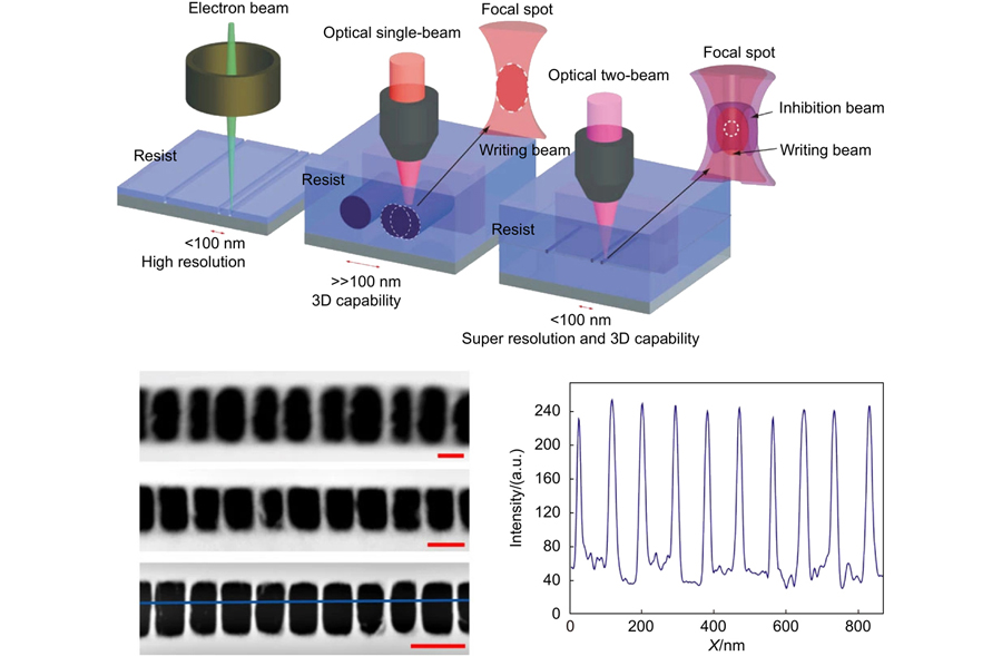
Therefore, in this review, the principle and advantages of femtosecond laser as well as its application in the micro/nano processing of optical device are discussed in detail. This review is divided into five sections. The first section introduces the mechanism and processing properties of femtosecond laser. The second section discusses a variety of methods to improve the resolution of femtosecond laser micromachining. The third section focuses on the femtosecond laser processing technology, and the fourth section describes the femtosecond laser's application in the processing of optical devices, including microlens, optical waveguide, grating, and photonic crystals. Finally, this review makes a summary and discusses the prospect of femtosecond laser micromachining used in optical devices.
飞秒激光 高精度 微纳结构 光学器件 femtosecond laser high-precision micro/nano structure optical device 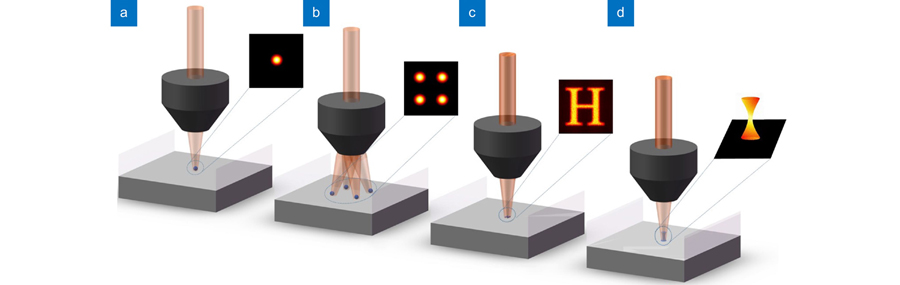
Overview: Two-photon lithography (TPL) has been a research hotspot in 3D micro/nano writing technology due to its characteristics of high resolution, low thermal influence, a wide range of processed materials, low environmental requirements, and 3D processing capability. It has shown unique advantages in the fields of life science, material engineering, micro/nano optics, microfluidic, micro machinery, and so on. This paper summarizes the research works done by researchers on different writing methods to improve TPL processing efficiency. Single-beam writing is the main method for TPL, which mainly depends on the speed of the scanning device. Single-beam writing has the advantages of simple system and high-quality beam, and it is easy to combine various effects to improve writing results. It mainly includes scanning modes based on the translation stage, galvo, polygon laser scanner, and acousto-optic deflector (AOD) (Fig. 2 ). All these modes have advantages and disadvantages. As for the scanning speed comparison, polygon laser scanner and AOD have relatively faster writing rates (faster than m/s). Multi-foci parallel lithography can obviously promote efficiency, elevating the speed by dozens or even hundreds of thousands of times, mainly based on spatial light modulator (SLM), digital micromirror device (DMD), microlens array (MLA), diffractive optical elements (DOE), multi-beam interference, and so on (Figs. 3- 15 ). Multi-foci parallel lithography based on SLM is most widely used owing to its high efficiency and ability to flexible and independent control of each single beam, but the refresh rate is still insufficient. DMD has a higher refreshing rate (32 kHz), but the state-of-the-art beam parallelism realized by DMD is severely limited. More parallel beams are further required for improving the processing efficiency. The 2D pattern exposure method based on SLM or DMD can further improve the TPL efficiency with the superiority of generating flexibly designed pattern (Figs. 16- 18 ). However, the 2D projection exposure technology is still difficult to achieve high writing precision, especially the axial resolution. An available method to improve the axial precision is spatially and temporally focusing an ultrafast laser to implement a strong intensity gradient at the spatial focal plane that restricts polymerization within a thin layer. The 3D projection method will be the most efficient writing method in the future, especially in 3D device processing (Figs. 19- 20 ). Researchers used this technique to make hollow tubular and conical helices structures, increasing the processing speed by 600 times. However, the research results show that the current 3D projection can only process simple 3D structures. Further researches on 3D exposure processing of complex structures are expected, which will effectively expand its application in various fields. Authors believe that with the effort of researchers on efficiency improvement gradually, TPL can further highlight its advantages to promote the development of life science, materials engineering, micro-nano optics, and many other fields.
飞秒激光直写 双光子光刻 单光束扫描 多焦点并行 面曝光 体曝光 femtosecond laser direct writing two-photon lithography single-beam scanning multi-focus parallelism pattern projection 3D projection exposure 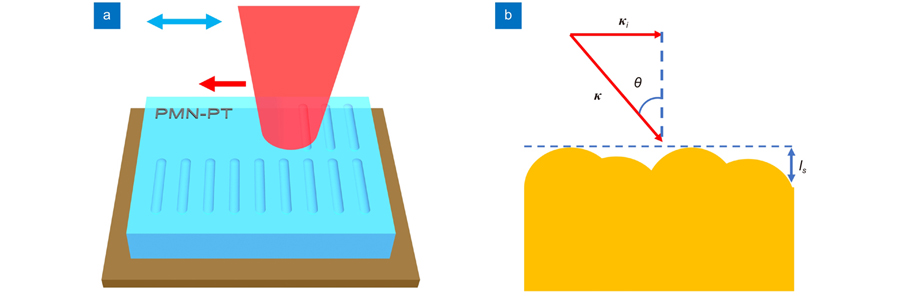
Overview: With the development of modern manufacturing, the size of optical devices is gradually developing towards miniaturization, and integrated optics is also developing to become a topical area of research for many scholars. One of the methods used for producing micro/nano optical devices is femtosecond laser direct writing, a fine three-dimensional processing technique that has been extensively studied by many scholars for its applicability to most materials and can be applied to the fabrication of a wide range of optical devices. Micro/nano-optical devices prepared by femtosecond laser direct writing in crystals have been applied in a broad range of applications in different wavelengths. PMN-PT crystal with relaxed ferroelectric has attracted much attention in recent years for its superior piezoelectric property and large electromechanical coupling coefficient, and its application in the infrared band is more prominent, so the fabrication of the optical devices based on PMN-PT crystal has gradually become a relevant research hotspot. The LIPSS is one of the micro/nano-structures that can be processed by femtosecond laser direct writing. The LIPSS is prevalent in many materials and has been found in metals, semiconductors, dielectrics, etc. Similarly, LIPSS can be induced by femtosecond lasers in PMN-PT crystal. The LIPSS has a wide range of applications in the fields of anti-reflectivity, permanent coloration, and wettability. Nevertheless, the physical processes and the mechanisms involved in the formation of LIPSS have different interpretations in different materials. In this paper, we describe the LIPSS induced by femtosecond laser on the surface of the PMN-PT crystal and characterize it theoretically. We have achieved a change in the period of the LIPSS from 750 nm to 3000 nm after experimenting with different laser parameters. Afterward, we simultaneously obtained the phase transition of the LIPSS in PMN-PT crystal through temperature modulation, and this phase transition can be analyzed by the variation of the Raman spectra. At the same time, we have obtained the Curie temperature for the LIPSS structure that is approximately 10 ℃ lower than that of the PMN-PT crystal and have analyzed the phase transition process through the structural properties of the PMN-PT crystal. The results of our experiments and analyzes on the LIPSS in PMN-PT crystal reported in this paper can provide some experience for the subsequent development of the optical devices related to the LIPSS in PMN-PT crystal.
飞秒激光直写 表面周期结构 PMN-PT晶体 相变 femtosecond laser direct writing LIPSS PMN-PT crystal phase transition 
Finally, the limitations of laser processing at present are summarized, and the application and development of laser micromachining technology in the field of medical equipment in the future are prospected. Although laser microprocessing technology can micro-process a new generation of implantable medical devices with extremely fine structure, making the commercial use of the next generation of implantable medical devices feasible, the development of laser micro-processing technology in the biomedical field is not mature enough, the production efficiency is low, and the work stability needs to be improved. For the laser micromachining process, a complete set of theories has not yet been formed to explain the physical nature of the interaction between the laser and material under the extreme conditions of ultra-fast, ultra-short, and ultra-strong, nor can the impact of laser micromachining on the material structure and physical and chemical properties be well evaluated. The next work still needs a lot of basic and regular research. At the same time, according to the characteristics of laser micromachining and the properties of the processed materials, it is also necessary to develop simulation analysis software to simulate the micromachining process and optimize the parameters of the laser micromachining process.
激光微细加工 血管支架 骨支架 生物材料 抗菌性 laser micromachining vascular stent bone stent biological materials antibacterial 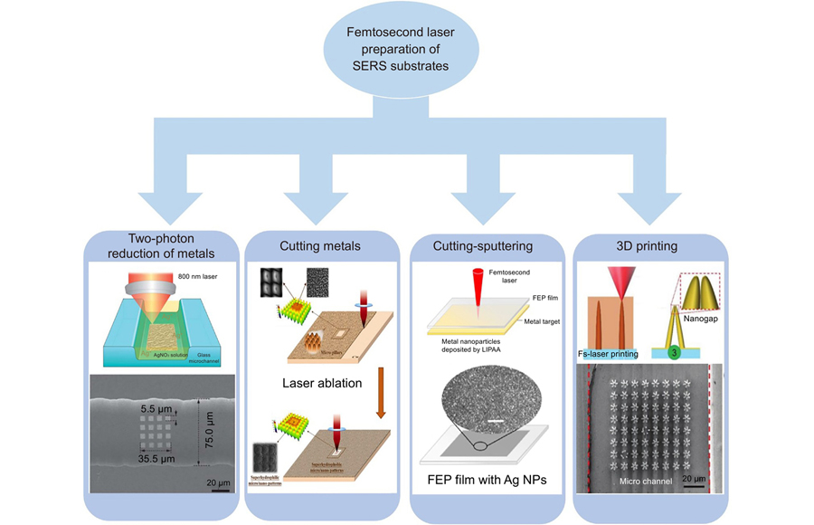
Overview: Surface-Enhanced Raman spectroscopy (SERS) is a highly sensitive and high-resolution molecular recognition technique with important applications in many fields. As an emerging low-cost, high-resolution, and highflexibility micro-nano processing method, femtosecond laser direct writing has been widely used in the field of preparing SERS substrates. Compared with traditional processing methods for preparing SERS substrates, femtosecond laser direct writing processing has certain advantages in terms of flexibility, three-dimensional molding, processing material range, processing accuracy, and other aspects. In this review, we classify the processing methods of femtosecond laser preparation of SERS substrates into four categories, including femtosecond laser two-photon metal reduction, femtosecond laser cutting metal, femtosecond laser cutting-sputtering, and femtosecond laser 3D printing. Femtosecond laser two-photon metal reduction uses the two-photon reduction effect to reduce metal cations in metal solutions to metals, such as silver ions in silver nitrate solutions to silver nanoparticles. This method is suitable for the one-step preparation of SERS substrates in closed microchannels. Femtosecond laser cutting metal directly prepares the SERS substrate structure on a metal substrate. This method takes advantage of the high peak power of the femtosecond laser to ablate the surface of the metal sample to obtain a patterned surface structure. At the same time, femtosecond laser ablation produces particle fragments, which are usually redeposited on the patterned surface, resulting in SERS "hot spots". Femtosecond laser direct cutting of metal can prepare SERS substrates in one step, which has the advantages of high processing efficiency and simple processing and is more conducive to the application of large-scale production of practical SERS detection. Femtosecond laser cutting-sputtering is to process any structure on non-metallic substrates such as polymers and then sputtering/evaporating metal nanoparticles on the surface of the structure. This method can prepare transparent and flexible SERS substrates, which are rich in application scenarios. Femtosecond laser 3D printing is to use the three-dimensional processing ability of femtosecond lasers to obtain rich "hot spots" by designing the structure of SERS substrates, and then using template-guided self-assembly technology with different driving forces to deposit/evaporate metal nanoparticles at designated locations. In this paper, we first introduce the current methods for preparing SERS and then conduct a comprehensive review of the processing methods of four femtosecond lasers to prepare SERS substrates. Finally, the advantages and disadvantages of the four femtosecond laser preparation methods for SERS substrate are briefly summarized, and the development prospects of this technology are prospected, aiming to provide it for future related research.
表面增强拉曼光谱 飞秒激光直写 微纳加工 SERS基底 SERS femtosecond laser direct writing micro/nano processing SERS substrate 
Such as, by using the photothermal effect of materials, the surface tension of the lubrication layer on the surface of materials can be changed, thus creating a wetting gradient force to push the droplets to move. Further, the sliding and pinning of the droplet can be controlled by the phase change of the paraffin layer on some functional surfaces. The pyroelectric crystal can generate the dielectric force field on its surface based on the photothermal effect, which could be applied to realize the lossless moving, merging, and splitting of the droplets. In addition, the wettability of the photovoltaic crystals could be changed with the irradiation of light, therefore, can be used to control the behavior of droplets. In this paper, the development of the photo-responsive functional surface in droplet manipulation was briefly reviewed. The mechanisms of the droplet manipulation with the functional surface were expatiated. The categories of functional surfaces were summarized, the characteristics of the structure were analyzed, and the corresponding implementation method was introduced in detail. In addition, the applications of the photo-responsive functional surface in droplet transportation, fusion, and segmentation were introduced. Finally, the future development and potential applications of the photo-responsive functional surface for droplet manipulation were prospected.
光响应 功能表面 液滴操控 润湿性 photo-responsive functional surface droplet manipulation wettability 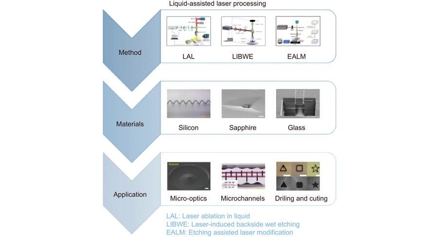
Overview: With the development of industry, laser fabrication has become one of the important technologies for welding, cutting, surface processing, and other advanced manufacturing areas. At the same time, the pursuit of structures miniaturization, devices integration, and high precision has put forward more stringent requirements for laser fabrication technologies. Due to the advantages of stable mechanical and chemical properties and unique photoelectric properties, hard and brittle materials have been widely used in aerospace, the photoelectric industry, et al. Laser fabrication is an ideal technology for hard and brittle materials processing due to its high precision, high energy, and non-contact properties. In order to achieve the removal of hard and brittle materials, high laser energy is usually required, resulting in low fabrication accuracy and poor surface quality. As an improved laser processing method, liquidassisted laser fabrication can effectively improve fabrication accuracy and surface quality. The processing characteristics and material removal principles of three different liquid-assisted laser processing technologies are summarized in this review. According to the different functions of the medium through which the laser penetrates and the kinds of liquid, liquid-assisted laser fabrication technology can be divided into Laser ablation in liquid (LAL), laser-induced backside wet etching (LIBWE), and etching-assisted laser modification (EALM). The auxiliary liquid of Laser ablation in liquid is mostly water, which mainly plays the role of cooling and removing debris. The auxiliary liquids used by laser-induced backside wet etching include organic solvents, acid-base solutions, inorganic salts, and other liquids, which play different roles according to different liquids. The etching-assisted laser modification mainly uses an acid or alkaline solution as an auxiliary liquid to remove laser-modified materials. Different methods and auxiliary liquids have different mechanisms in the methods. Therefore, almost any material can be processed by choosing suitable methods and auxiliary liquids, including photosensitive glass, silicon crystal, sapphire, and other transparent hard brittle materials. Here, we summarize the fabrication technologies and fabrication parameters for different materials. The development and applications of liquid-assisted laser fabrication technologies in the fields of micro-optical components, microfluidic devices, and drilling and cutting are introduced. Finally, the challenges of the technology are discussed.
激光加工 硬脆材料 液体辅助制造 微/纳米结构 laser fabrication hard and brittle materials liquid assisted fabrication micro/nano structures 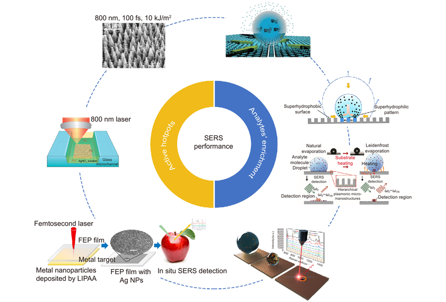
Overview: Surface-enhanced Raman scattering (SERS) affords a rapid, highly sensitive, and nondestructive approach for label-free and fingerprint diagnosis of a wide range of chemicals. This technique has been applied in explosives detection, pre-cancer diagnosis, food safety, and forensic analysis, where a small number of hazardous substances can seriously affect health of human beings. Thus, it is of great significance to prepare high-performance SERS sensors. In general, the signal intensity of SERS is determined by the following three factors: 1) The enhancement effect of surface nanostructure on local electric fields; 2) The number of molecules to be detected in hot spots; 3) Performance of the Raman spectrometer. Therefore, in order to achieve high-performance SERS detection of trace molecules, current research focuses on how to increase the density of hot spots and the number of analyte molecules in the detection area. An ultrafast laser has an ultra-short pulse width and ultra-high peak power, so it can interact with the majority of materials with high processing accuracy and excellent controllability. Meanwhile, it can rapidly construct a variety of large-area micro/nano-structures on material surfaces based on facile digital programming strategies. In addition, combined with multi-beam parallel fast scanning technology, low-cost and high-efficiency machining can be realized without a special requirement for the machining environment. Based on the above advantages, the ultrafast laser has become one of the important means for the fabrication of micro/nano-structures. This is important for the commercial preparation of high-performance SERS sensors. In this paper, we focus on two aspects to introduce the ultrafast laser preparation of high-performance SERS sensors, including how to increase the density of hot spots and the number of analyte molecules in the detection region. Ultrafast lasers can prepare micro/nano-structures with local field enhancement effects by both "bottom-up" and "top-down" processing strategies. The first is based on the "bottom-up" principle, where the reduction, deposition or polymerization of atoms, molecules or other nanoparticles is controlled by ultrafast lasers to achieve additive manufacturing of micro/nano-structures. The other is based on the "top-down" principle, where materials are removed by the ultrafast laser ablation to rapidly achieve hierarchical micro/nanostructures. These structures provide abundant active hot spots for SERS detection. In particular, the superhydrophobic surfaces prepared by the ultrafast laser are one of the most effective methods to achieve the enrichment of analyte molecules. Raman scattering can be excited more effectively by enriched molecules, which is conducive to obtaining higher detection limits and realizing ultra-trace detection. Finally, a prospect for the development of laser-prepared SERS substrates is provided.
超快激光加工 拉曼光谱 表面增强拉曼散射 微纳结构 ultrafast laser fabrication Raman spectroscopy surface-enhanced Raman scattering micro/nano-structures