Photonics Research, 2019, 7 (8): 08000B48, Published Online: Jul. 12, 2019
Magnesium ion-implantation-based gallium nitride p-i-n photodiode for visible-blind ultraviolet detection  Download: 929次
Figures & Tables
Fig. 1. (a) Schematic diagram of Mg ion implantation in GaN. (b) SIMS results of Mg distribution in the GaN layer before and after annealing. (c) 2 θ

Fig. 2. (a) Current-voltage (I-V ) characteristics of the fabricated quasi-vertical GaN p-i-n diode with a Mg implanted p-type layer; the inset illustrates the cross-sectional schematic of the diode. (b) I-V results in linear plots. (c) Electroluminescence (EL) spectrum of the Mg ion-implanted GaN p-i-n diode; the inset displays the EL emission pattern.
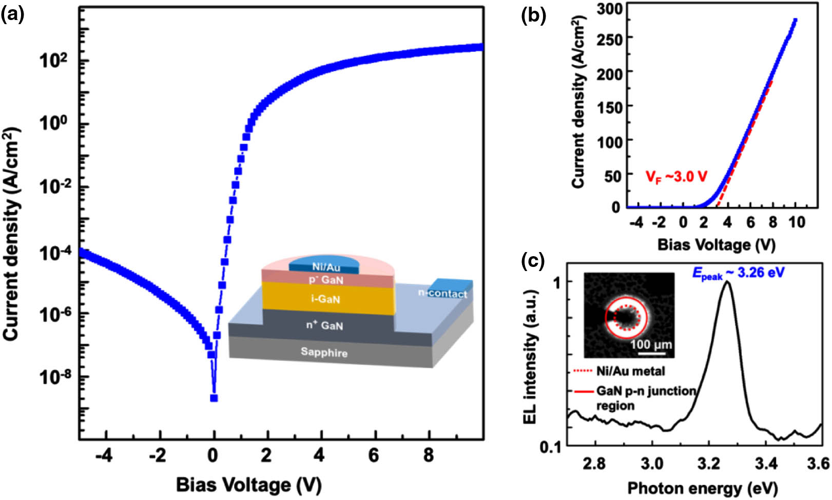
Fig. 3. (a) Photo- and dark current measurements for the Mg ion-implanted quasi-vertical GaN p-i-n photodiode. (b) Spectral response characteristics at zero bias of the UV photodetector based on the Mg ion-implanted p-i-n diode (blue) and a commercially available GaN p-n photodiode (red).

Fig. 4. (a) Temperature-dependent leakage measurement. (b) Hopping conducting-based linear fitting between ln ( J ) E α 1 / T 5 / 4 ln ( J ) E 1 / 2

Fig. 5. (a) Reverse-bias-dependent responsivity measurement at an optical power density of 2.5 mW / cm 2


Weizong Xu, Yating Shi, Fangfang Ren, Dong Zhou, Linlin Su, Qing Liu, Liang Cheng, Jiandong Ye, Dunjun Chen, Rong Zhang, Youdou Zheng, Hai Lu. Magnesium ion-implantation-based gallium nitride p-i-n photodiode for visible-blind ultraviolet detection[J]. Photonics Research, 2019, 7(8): 08000B48.


 PDF全文
PDF全文

