Black silicon (BS) is widely researched in the areas of photodetectors, solar cells, and sensors since it has many remarkable properties, such as a large absorption range and a highly effective surface area[1–5" target="_self" style="display: inline;">–5]. When its micro/nano-roughened surface is coated with metal nanoparticles, BS could be utilized for various other applications, such as surface-enhanced Raman scattering (SERS) sensors[68" target="_self" style="display: inline;">–8]. For instance, silver-covered BS with nanopillar forests could work as a SERS active biosensor[9]. The above metal BS systems were mainly prepared by physical methods such as magnetron sputtering[10] or evaporation[9,11]. In this Letter, for the first time to our knowledge, a chemical growth method to grow silver nanoparticles (AgNPs) on BS on a microfluidic chip is reported. Compared with earlier works, the chemical growth approach here has important advantages, including site-selectivity and probable higher stability via stronger affinity. The BS substrate was fabricated in the atmosphere of sulfur hexafluoride () by nano-precision, mask-free, and noncontact femtosecond laser direct writing (FsLDW)[12–24" target="_self" style="display: inline;">–24]. Hydrofluoric acid (HF) was used to remove the oxide layer on the surface of the BS and to passivate it by hydrogen, which increased its reducing reactivity[25,26]. Then, the wafer was immersed into a silver nitrate solution () to prepare the Ag-BS micro/nano-structures. The parameters influencing the growth of AgNPs were studied, and the Ag-BS functionalized chip was prepared to undergo a microfluidic catalytic reaction and SERS detection. Also, the arrays of Ag-BS composite devices might help to sufficiently mix p-nitrosophenol (pNP) and sodium borohydride (). The detection limit was characterized by Rhodamine 6G (R6G) to be .
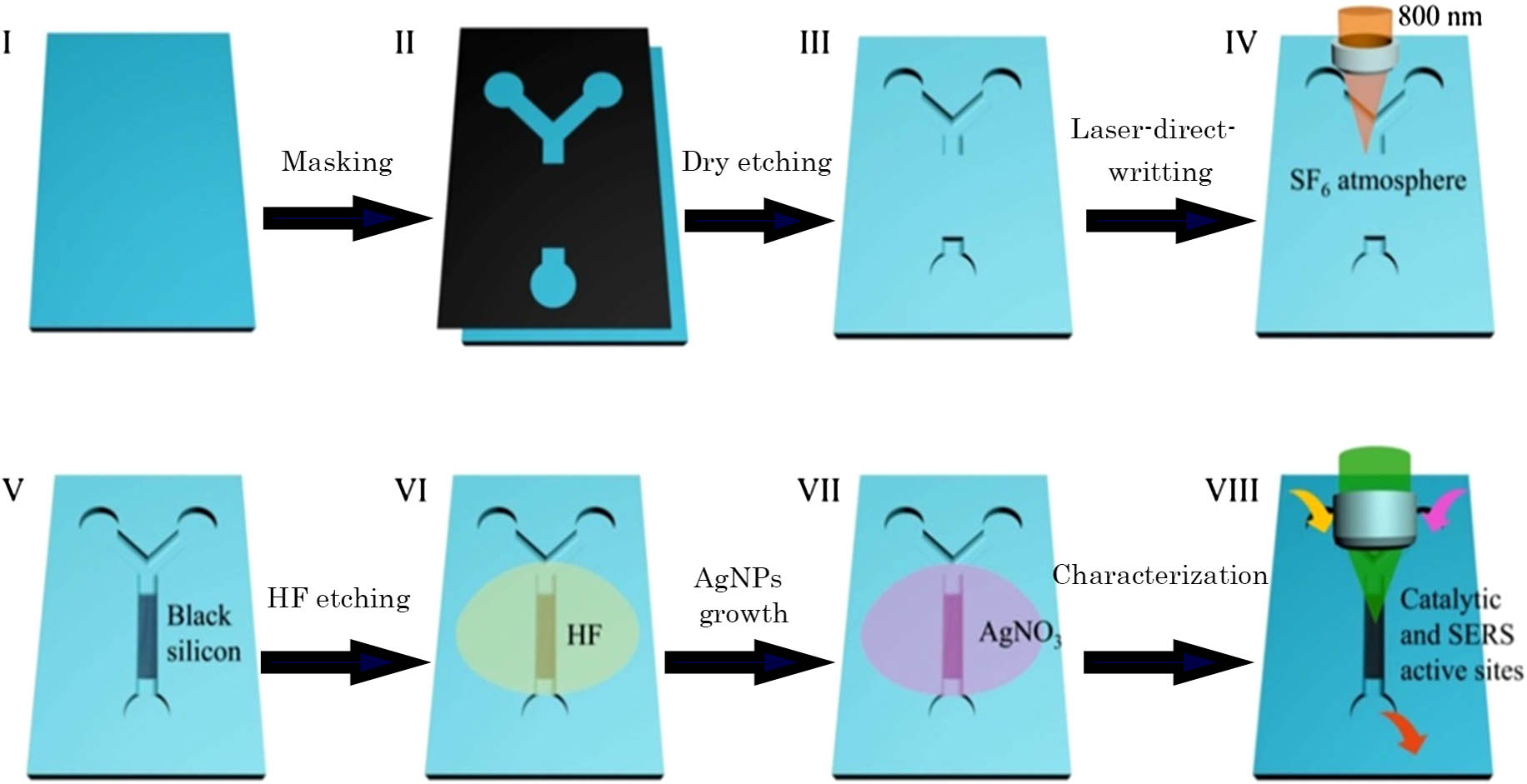
Figure 1 shows the scheme of the fabrication process. As illustrated in I–III in Fig. 1, a “Y” shape microfluidic channel with a 1 cm-long non-etched part was fabricated on a silicon wafer using dry etching[25]. The channel was about 200 μm in width and 20 μm in depth. The BS arrays were then patterned on the non-etched part by FsLDW, as illustrated in IV and V. The FsLDW process was conducted in a sealed chamber filled with at a pressure of 0.07 MPa. The 800 nm femtosecond laser pulses used here were generated by a Ti:sapphire regenerative amplifier laser system (Spectra Physics). The laser pulse duration was 100 fs and the repetition rate was 1 kHz[27–34" target="_self" style="display: inline;">–34]. The laser power was 600 mW, and the scanning speed was . Before the AgNPs growth, the BS surface was treated with a 2% HF solution for 5 min to remove the oxide layer (step VI), and then immersed into solution. The silver ions were reduced into silver and attached on the surface of the BS, as shown in VII. Finally, the catalytic reaction and SERS detection are carried out on the Ag-BS area, as shown in step VIII. The reduction of pNP to p-aminophenol (pAP) by was chosen as a model reaction for both the on-chip catalytic test and the in-situ SERS detection[35,36]. and pNP were injected into two branches of the “Y”-shaped channel. The reduction started when the two reactants mixed together in the Ag-BS area. In-situ SERS detection was then carried out, which could evaluate the reduction process of pNP to pAP. The SERS were recorded on a LabRAM HR Evolution (from HORIBA Scientific) equipped with an He–Ne laser at 633 nm as an excitation source. The laser power was about 1 mW, and the average spot size was 1 μm in diameter.
Fig. 1. Schematic illustration of the experiment. (I–III) Microfluidic chip fabrication on Si wafer by dry etching. (IV–V) BS fabrication by laser. (VI) HF treatment on BS. (VII) AgNPs’ growth on BS. (VIII) Catalytic reaction and SERS detection on Ag-BS substrate.
下载图片 查看所有图片
After step V in Fig. 1, the morphology of the BS was checked by a scanning electron microscope (SEM). The SEM images and energy dispersive spectrometer (EDS) spectra were taken by a field emission SEM/EDS (FESEM/EDS, JSM-7500F, JEOL, Japan). As shown in Fig. 2, the surface presented a quasi-ordered arrangement of micro-pointed cones with a height of about 18 μm. When utilized as a catalyst template, these micro-pointed cones would greatly increase the effective contact area between the reactants and catalysts. When combined with metal nanoparticles, the nanoscale-roughened surface [Fig. 2(a)] would help to generate localized surface plasmon polaritons (LSPPs) to enhance the electromagnetic field.
Fig. 2. SEM images of the BS with (a) side view and (b) oblique view.
下载图片 查看所有图片
Figure 3 shows the SEM images of AgNPs’ morphology on different parts of the BS protrusions. The AgNPs on the top [Fig. 3(b)] were larger and distributed more densely. The sizes of the AgNPs were about 200, 50, and 10 nm at the top, middle, and bottom positions of the protrusion, respectively [Figs. 3(b)–3(d)]. The reason for this is that the chemical potential of the top position was larger than that of the other parts, so when it was immersed in the solution, the top surface would be more active and reduce more AgNPs.
Fig. 3. (a) SEM image of the AgNPs on the BS protrusions. (b), (c), and (d) Enlarged SEM images of AgNPs on the area marked by red, green, and blue squares in (a).
下载图片 查看所有图片
High temperature could promote the growth of the AgNPs. In order to get an optimized temperature, we examined the AgNPs’ growth under four different temperatures, as shown in Fig. 4. At 15°C, the size of the nanoparticles was relatively small (1–2 nm). At the increased temperature of 25°C and 50°C, the nanoparticles size increased to 20 and 50 nm, respectively. As the temperature reached 75°C, the AgNPs became larger than 100 nm, and the shape became irregular rather than spherical. As the larger and irregularly shape AgNPs are not useful for catalysis, we chose the room temperature (25°C) for the AgNPs’ growth.
Fig. 4. SEM images of the AgNPs grown under (a) 15°C, (b) 25°C, (c) 50°C, and (d) 75°C. The scale bars indicate 100 nm.
下载图片 查看所有图片
The solution concentration could also affect the growth of the AgNPs. In this section, four different concentrations of solution were used to optimize the AgNPs’ growth. As shown in Figs. 5(a)–5(d), when the concentration was down to 0.001 M, the size of the nanoparticles was rather small (), and they spread over the surface of the BS sparsely. As the solution concentration increased, both the nanoparticles’ size and density became larger. However, when the concentration reached 1 mol/L [Fig. 5(d)], the nanoparticles became too large and presented more like a block shape with fewer gaps, which was not suitable for either catalysis or LSPPs generation. We therefore chose 0.1 mol/L as the best concentration of solution.
Fig. 5. SEM images of the AgNPs grown in (a) 0.001, (b) 0.01, (c) 0.1, and (d) 1 mol/L solution. The scale bars indicate 100 nm.
下载图片 查看所有图片
Figure 6 shows EDS spectra of the Ag-BS structures. The strong energy peak of Ag indicates the existence of the silver element on the BS surface. As illustrated in the insets of Figs. 6(a) and 6(b), the silver content increases with the reaction temperature and the solution concentration, which accord well with the previous discussion.
Fig. 6. EDS spectra of the Ag-BS (a) under different reaction temperatures, where inset shows the peak intensity versus temperature; and (b) with different solution concentrations, where inset shows the peak intensity versus concentration.
下载图片 查看所有图片
The SERS spectra were used to monitor the microfluidic catalytic reaction[35,36]. The black and red curves in Fig. 7 represent the SERS spectra of pNP and pAP taken before and after the catalytic reaction of pNP reduced to pAP, respectively. The Raman mode at in the SERS spectrum before the reaction is the peak of nitro-bonding to the benzene ring in the pNP molecule. After the reaction, two distinct Raman modes at 1275 and were clearly observed, which represented the peak of amino-bonding to the benzene ring in the pAP molecule (see inset of Fig. 7). Judging by the Raman spectra changes, it was easy to monitor the chemical reaction process. Here, the BS’s protrusions helped to accommodate the Ag nanoparticles packed in with a high surface area, which made them good candidates as active catalytic sites. Also, the Ag-BS substrate proved its potential for in-situ SERS detection.
Fig. 7. SERS spectra taken before (black line) and after (red line) the catalytic reaction of pNP to pAP. Inset illustrates the chemical reaction process.
下载图片 查看所有图片
By using R6G as a probe molecule, the SERS activity of the silver-BS substrate was studied. The SERS spectra of the R6G with concentrations of are shown in Fig. 8. Distinct peaks[37] with a high signal-to-noise (S/N) ratio were clearly observed, even for the concentration as low as . It indicated that the Ag-BS substrate has a large Raman enhancement. Considering the S/N ratio and reproducibility, the detection limit was concluded to be at (an even lower concentration could be detected). The strong SERS enhancement can be explained by the dramatically enhanced electromagnetic field on the rough distributed AgNPs on the BS substrate[7]. Importantly, the catalytic reactors themselves (hierarchically, micro/nano-structurised Ag-BS composite devices) worked as the SERS sensors for the chemical reaction and analysis at the same time, which might be of great help to improve the microfluidic chip integration.
Fig. 8. SERS spectra of R6G with the concentrations ranging from to .
下载图片 查看所有图片
In conclusion, hierarchically micro/nano-structured Ag-BS composite devices are in-situ constructed and integrated in a microfluidic chip simultaneously for catalytic reaction and SERS-based monitoring. The BS substrate is femtosecond-laser fabricated in the atmosphere of SF6. It is then etched and hydrogenated using a HF solution for the templated chemical growth of AgNPs. Comprehensively considering SERS sensing and catalytic efficiency, optimized parameters of AgNPs growth are applied to obtain an average diameter and dense loading with gaps (room temperature 25°C and 0.1 mol/L solution concentration). The microfluidic chip, functionalized with hierarchically micro/nano-structurized Ag-BS composite devices, is prepared for a catalytic reaction (pNP to pAP) in microfluidics. Meanwhile, these Ag-BS composite devices themselves function as in-situ SERS sensors to monitor the reaction processes. The SERS-detection limit is determined to be better than by using R6G as a probe sample. As a “generalist” of both catalytic reactors and SERS sensors, the hierarchically micro/nano-structurised Ag-BS composite devices here may open new opportunities for various applications like highly integrated chemical synthesis and analysis, and biomedical sensing and diagnosis.
Zhaoxu Yan, Chunhao Li, Yang Luo, Jihong Zhao, Hai Yang, Prabhat Verma, Satoshi Kawata . Silver hierarchical structures grown on microstructured silicon in chip for microfluidic integrated catalyst and SERS detector[J]. Chinese Optics Letters, 2015, 13(10): 102401.
 Download: 1112次


