光学学报, 2020, 40 (10): 1031001, 网络出版: 2020-04-28
周期性微结构对红外场景生成芯片空间分辨率的影响  下载: 992次
Spatial Resolution of Infrared Scene Projector Chip with Periodical Microstructure
图 & 表
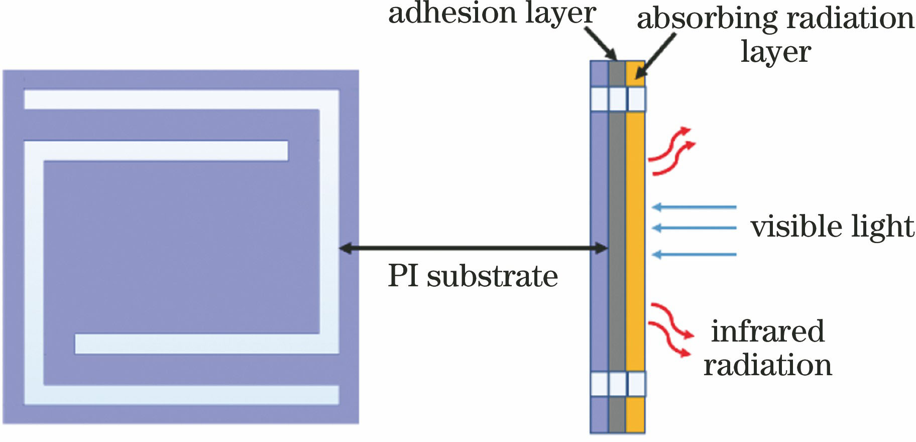


图 5. 具有周期性微结构的MEMS芯片的温度分布计算模型
Fig. 5. Temperature distribution calculation model of MEMS chip with periodical microstructure


图 8. 用于接触面积比分析的微结构示意图。(a)微结构平面图;(b)微结构立体图
Fig. 8. Schematic of microstructure used for contact area ratio analysis. (a) 2D diagram of microstructure; (b) 3D diagram of microstructure

图 9. 不同接触面积比时芯片表面沿x方向的辐射强度分布
Fig. 9. Thermal radiation intensity distributions along x-direction of chips with different contact area ratios

图 10. 具有不同接触面积比的周期性微结构芯片的MTF曲线
Fig. 10. MTF curves of microstructured chips with different contact area ratios

图 11. 用于填充因子分析的微结构示意图
Fig. 11. Schematic of microstructure used for filling factor analysis

图 12. 具有不同填充因子的微结构芯片的辐射强度分布
Fig. 12. Thermal radiation intensity distributions of microstructured chips with different filling factors

图 13. 具有不同填充因子的微结构芯片的MTF曲线
Fig. 13. MTF curves of microstructured chips with different filling factors

图 14. 红外场景生成芯片的周期性面内微结构示意图。(a)接触面积比为0.20;(b)接触面积比为0.46
Fig. 14. In-plane microstructures of infrared scene projector chips. (a) Contact area ratio of 0.20; (b) contact area ratio of 0.46


图 16. 周期性微结构的显微镜图像。(a)接触面积比为0.2;(b)接触面积比为0.46
Fig. 16. Microscope images of periodical microstructure. (a) Contact area ratio of 0.2; (b) contact area ratio of 0.46


图 18. 红外热像仪采集到的结果。(a)芯片表面辐射分布图;(b)沿x轴方向的温度分布曲线
Fig. 18. Measurement results obtained by infrared thermal imager. (a) Thermal radiation intensity distribution on chip surface; (b) temperature distribution along x-direction

图 19. 两个芯片样品沿x轴方向的辐射强度分布曲线
Fig. 19. Radiation intensity distribution curves along x-axis of two chip samples


赵乾, 李卓, 王欣, 李德芳, 徐立强. 周期性微结构对红外场景生成芯片空间分辨率的影响[J]. 光学学报, 2020, 40(10): 1031001. Qian Zhao, Zhuo Li, Xin Wang, Defang Li, Liqiang Xu. Spatial Resolution of Infrared Scene Projector Chip with Periodical Microstructure[J]. Acta Optica Sinica, 2020, 40(10): 1031001.


 PDF全文
PDF全文

