As one of the most useful materials, germanium (Ge) films are frequently used in the optical and photonic industries for solar cells and photo-thermal applications[1–6" target="_self" style="display: inline;">–6]. Ge films have much attractive attention owing to their lower optical band gap energy and higher mobility as compared to Si[7]; moreover, with the development of infrared optical technology, Ge not only can be used as one of the excellent infrared window materials, but also can be used as a high refractive index material in multilayer interference coatings for the infrared range[8–13" target="_self" style="display: inline;">–13].
In view of the urgent need for multi-wavelength common windows in military applications in the future, which requires film with high transmittance in visible (Vis), near-infrared (NIR), mid-infrared, and even far-infrared, while requiring film with excellent protection in extreme environments, diamond-like carbon (DLC) films[14] and [15] materials with excellent protection have been used as an infrared window protection layer. However, the internal stress of the layer and the adhesion to the substrate are crucial issues, which may induce the films to crack or even peel off. A simple and effective method to solve this problem is to deposit a buffer layer before depositing the hard protective films. Related literatures[16–19" target="_self" style="display: inline;">–19] report that Ge films can be used as an intermediate transition layer due to its good adhesion between the ZnS infrared window and some protective layer materials, such as DLC and . Previous studies on the optical properties of Ge films were usually focused on the films thicker than 100 nm[2022" target="_self" style="display: inline;">–22] and also at longer wavelengths ()[2325" target="_self" style="display: inline;">–25]. The research on the optical characteristics of ultrathin Ge films is still lacking.
In this paper, we presented three pieces of our work: (1) study the effects of different deposition temperatures (100°C, 200°C, and 300°C) on the optical properties of Ge films in the nanoscale regime (about 15 nm); (2) based on the high temperature annealing treatment at 500°C in air, roughly simulate the environment at high flight Mach numbers and then analyze the effect of high temperature on the optical characteristics of Ge films; (3) based on the model proposed by Wang et al.[26], a reasonable interpretation of optical band gap changes is given.
The Ge films were deposited on fused quartz substrates at different deposition temperatures by electron beam evaporation with argon plasma assistance. During the preparation of Ge films, the deposition rate was kept at 0.2 nm/s, the base pressure was kept at , and the deposition pressure was kept at . The thickness was controlled by a quartz crystal monitor, and the value of the tooling factor was set to a constant at three different deposition temperatures. The annealing treatment was carried out in air (1 atm) at 500°C for a fixed time of 2 h, and the rate of heating and cooling was kept at 3°C/min. The crystal structure of Ge films was characterized by X-ray diffraction (XRD), and the thickness of Ge films before and after the annealing treatment was measured and fitted by grazing incidence X-ray reflectivity (GIXRR), performed on a PANalytical Empyrean reflectormeter with (0.154 nm) radiation. To examine the amorphous degree of the Ge thin films, Raman spectroscopic measurement was conducted using the Renishaw InVia Raman spectrometer (Renishaw Ltd., UK) with the 488 nm line laser. The optical transmittance of Ge films before and after annealing treatment was measured by a Cary 5000 UV-Vis-NIR spectrophotometer and LZH ML6500 vacuum UV (VUV) spectrophotometer. The surface and interface compositions were analyzed by a Thermo Scientific X-ray photoelectron spectroscopy (XPS) instrument equipped with a monochromatic Al X-ray source.
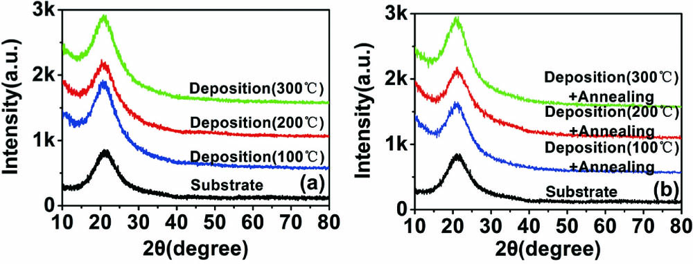
Figure 1 shows the XRD pattern of Ge films before and after annealing treatment. All of the films are amorphous, as indicated by the broad low-intensity hump. The peak around represents the amorphous peak, which is mainly caused by the amorphous structure of the quartz substrate. Comparing Figs. 1(a) and 1(b), there is no significant difference between the Ge films before and after annealing: all peaks are similar to the quartz substrate, indicating that the films are amorphous. The XRD results are in agreement with the studies by Khan et al.[27] regarding the annealing treatment of nanostructure Ge films on BK7 glass substrates.
Fig. 1. X-ray diffraction patterns of Ge films: (a) before annealing, (b) after annealing.
下载图片 查看所有图片
In order to examine the amorphous degree of the Ge films before and after annealing, the Raman spectra are shown in Fig. 2. Peak separation has been performed by curve fitting, and a broad Raman band at around is observed for all samples before annealing, which is similar to that of amorphous Ge (-Ge) films[28,29]. Another Raman peak at about indicates that crystallization (Ge nanocrystals) has occurred[27,28]. The Raman peak is left shifted as compared to that for bulk Ge (), which is due to quantum confinement effects[27,30]. The position of the Raman peak related to scattering by optical phonons depends on the nanocrystal size; the larger the shift of the Raman peak towards smaller wave numbers with respect to the peak for the Ge bulk, the smaller the Ge nanocrystal size. By comparing the peak areas centered at and [shown in Figs. 2(a), 2(b) and 2(c)], it can be concluded that the amorphous structure of the film dominates. After annealing, in the wavenumber range, no peaks appear in the Raman spectra of all samples, and there is no significant difference from the spectra of the quartz substrate. According to the XPS test results, we speculate that this is related to all Ge elements in the films becoming . Combining the XRD pattern and Raman spectra after annealing, we deduce that the films are still amorphous.
Fig. 2. Raman spectra of Ge films: (a), (b), (c) before annealing, (d) after annealing.
下载图片 查看所有图片
Figure 3 shows the thickness of Ge films before and after the annealing treatment measured with the GIXRR method. The thickness of Ge films before annealing decreased almost linearly with increasing deposition temperature. According to the principle of quartz crystals to monitor the film thickness, the relationship between film thickness and quartz crystals vibration frequency can be expressed by , where is the film thickness, is the frequency constant of quartz crystal, is the density of quartz, is the resonant frequency of uncoated crystal, is the resonant frequency of loaded crystal, and is the density of film. Assuming the other parameters remain unchanged, it can be seen from this formula that the film thickness and density are inversely proportional. As the deposition temperature increases, the film density increases, so the Ge films thickness decreases. The optical transmittance and the optical band gap of the films before and after annealing treatment are shown in Figs. 4 and 5, respectively. After annealing, the thickness of all films increased compared with the thickness before annealing, but there is no obvious proportional relationship. The increase in film thickness after annealing can be explained from the diffusion between the films and the substrate. According to the results of XPS, shown in Fig. 6, we found that there is a wide transition region (etch time from ) between the films and the quartz substrate; the compositions are and . This is evidence of the existence of diffusion between the films and the substrate. Therefore, we believe that diffusion is responsible for the increase in film thickness after annealing.
Fig. 3. Thickness at different deposition temperatures: (a) before annealing, (b) after annealing.
下载图片 查看所有图片
In Fig. 4, the optical transmittance of Ge films before and after annealing treatment is displayed. The transmittance of the uncoated substrate was measured for comparison. It is worth noting that the shorter the wavelength, the greater transmittance attenuation of Ge films before annealing treatment, which is more significant with the deposition temperature increasing, as shown in Fig. 4(a). It is further noted that the transmission edge progressively shifted toward lower energy with increasing deposition temperature, which corresponds to the change in the optical band gap mentioned below. According to Luo et al.[31], the packing density of the Ge films increases as the deposition temperature increases. The relationship between the refractive index and packing density of the films can be expressed by the Kinosita formula: , where is the index of the material filling the voids, and is the index of the solid part of the films. It can be deduced from the Kinosita formula that the refractive index of the Ge films increases with the increase of the packing density. Under normal incidence, according to Fresnel reflection coefficient , it can be inferred that the greater the refractive index of the films, the greater the value of the reflection coefficient, the lower the transmittance value. As shown in Fig. 4(b), the transmittance of Ge films after annealing treatment is close to the transmittance of the uncoated substrate in the wavelength range of 600 to 2100 nm. Although the deposition temperatures of Ge films are different, the transmittance curves are almost coincident after the annealing treatment at 500°C, which can be explained by the increase in optical band gap caused by the oxidation of Ge films. After annealing in air at 500°C, Ge was oxidized to , which has a wider transparent band than Ge. As a result, the transmittance of the films samples increases significantly. In addition, comparing the XPS spectra of the films samples in Fig. 6, it was found that as the etching depth increases, the ratio of Ge/O/Si atomic concentration is basically the same. We believe that this is the fundamental reason why the transmittances of the film samples are basically the same.
Fig. 4. Transmittance of Ge films on fused quartz: (a) before annealing, (b) after annealing.
下载图片 查看所有图片
The optical band gap values of Ge films as-deposited and with annealing treatment are calculated by the extrapolated energy intercept of the Tauc plot. The Tauc equation is shown as follows[32]: where , , , and are the absorption coefficient, incident photon energy, proportionality constant, and optical band gap, respectively. In Eq. (1), the constant called the power factor of the transition mode is dependent on the crystalline or amorphous nature of the material and the type of electronic transition. The values for direct allowed, indirect allowed, direct forbidden, and indirect forbidden transitions are , 2, 3/2, and 3, respectively. For Ge films on the fused quartz substrate, . According to transmittance of Ge films samples, the absorption coefficient of Ge films can be obtained by using the equation [32] where is the film thickness, and is the transmittance. Combining Eqs. (1) and (2), the optical band gap energies of Ge films could be found by the linear extrapolation of to zero. Thus, the optical band gap before and after annealing can be obtained from Figs. 5(a) and 5(b), respectively. Before annealing, as the deposition temperature rises from 100°C to 300°C, the optical band gap decreases from 0.68 eV to 0.61 eV. In order to interpret the effect of deposition temperature, a Mott–Davis–Paracrystalline (MDP) model[26] is used. -Ge has a semiconductor-alloy-like structure, it may contain A [medium-range order (MRO)] and B [continuous network (CRN)] simultaneously, and there is a dependence of A/B ratio on film deposition temperature. The structure of -Ge can be defined as , and is the volume fraction of MRO. Considering that the thickness of Ge films prepared at three different deposition temperatures exceeds 15 nm, the MDP model formula mentioned can be simplified and described by Eq. (3): where is film thickness, and the critical value is only a constant determined by preparation conditions.
Fig. 5. Optical band gap of Ge films on fused quartz: (a) before annealing, (b) after annealing.
下载图片 查看所有图片
Fig. 6. XPS analysis of Ge films after annealing: (a), (d) deposition (100°C) + annealing, (b), (e) deposition (200°C) + annealing, (c), (f) deposition (300°C) + annealing.
下载图片 查看所有图片
The CRN structure of Ge films is dominant at deposition temperature of 100°C (), the MRO structure is considered to be dominant when the deposition temperature is 200°C and 300°C (), and the higher the deposition temperature, the higher the percentage of MRO. Pérez et al.[33] reported that the polycrystalline structure is present in Ge films prepared at 370°C. The reduction of the optical band gap is dependent on the strain exerted on topologically crystalline grains[34,35].
However, after annealing under the same conditions, the optical band gap is maintained at a large value (about 5.70 eV) with the deposition temperature rising from 100°C to 300°C. The optical band gap after annealing treatment is significantly increased compared with that before annealing. Some related research works[27] have been done to interpret the phenomenon. They attributed the reason to the formation of , but still lack accurate analysis results.
Oxidation can lead to an increase in the optical band gap of the Ge films after annealing. Khan et al.[27] discovered the Raman peak of and a single peak at assigned to Ge-O stretching vibration through Fourier transform infrared spectroscopy (FTIR) analysis for the films at 450°C and 500°C. Although the related literatures report that the Ge films are oxidized after high temperature annealing, information of in the depth direction is not given in detail. Therefore, the content of Ge films after annealing was analyzed by XPS depth profiling. Figure 6 shows the results of XPS analysis. By comparing the trend of atomic profiles under the three process conditions, the regular of Ge, Si, and O elements with etching time increasing is similar under different process conditions.
According to the position where the Si element appears, we can divide the atomic profile into regions A and B. For the process condition in Fig. 6(a), the boundary of regions A and B appears when the etch time is 120 s, and for process conditions in Figs. 6(b) and 6(c), the boundary of regions A and B appears when the etch time is 90 s. When the surface analysis was done by XPS (), the ratio value of Ge/O is 1/2 under three process conditions. It can be inferred that the compositions of the surface are . As the depth increases (etch time increases), the percentage of Ge atoms decreases () and then remains unchanged (etch time from 30s to the boundary of regions A and B). In region A, and GeO are the main compositions deduced by the ratio value of Ge/O. In region B (from the boundary of regions A and B to ), the main compositions are , GeO, and inferred by the ratio value of Ge/Si/O. Therefore, we believe that the reason for almost the same optical band gap of Ge films after annealing is the nearly identical compositions of films.
The optical properties of Ge films with thickness of about 15 nm on fused quartz substrates at different deposition temperatures were determined by a UV-Vis spectrophotometer. The results show that the transmittance of the films changes with the change of the deposition temperature, and the annealing treatment will significantly increase the transmittance in the range from 300 to 2000 nm. The analysis indicates that the optical band gap of Ge films decreased with deposition temperature increasing before the annealing, which can be well interpreted by the MDP model. After annealing, the band gap of Ge films that increased to ∼5.7 eV at different deposition temperatures (ranging from 100 to 300°C) was attributed to the formation of ( and GeO), which was analyzed by XPS. Both the deposition temperature and annealing treatment can alter the optical band gap of the Ge films to some extent, which enriches the optical band gap engineering.
Meng Guo, Hongbo He, Kui Yi, Shuying Shao, Guohang Hu, Jianda Shao. Optical characteristics of ultrathin amorphous Ge films[J]. Chinese Optics Letters, 2020, 18(10): 103101.
 Download: 824次


