1. INTRODUCTION
Silicon-on-insulator (SOI) microring resonators have attracted considerable attention for their potential applications in on-chip photonic systems for communication and sensing [1,2] due to their high quality factor and ability in spectral manipulation. However, silicon material itself possesses a large positive thermo-optic coefficient (TOC), , which is the main obstacle for microring resonators in many practical applications. Several methods aimed at eliminating or reducing the thermal effect on the microring resonators have been reported, such as integrating with heaters [3–6" target="_self" style="display: inline;">–6], cladding with negative TOC materials [7–11" target="_self" style="display: inline;">–11], utilizing broadband microrings [12], and coupling with Mach–Zehnder interferometers (MZI) [13,14]. Integrated heater is technically an active athermal scheme through feedback, thus limited by high tuning power consumption. Negative TOC materials require a certain amount of mode energy transferring in the cladding, therefore putting restrictions on waveguide geometric parameters and inducing higher propagation loss. MZI has relatively large footprint, inadequate for compact integration. Therefore, at present, the on-chip athermal microrings are still inaccessible and the essential requirements for on-chip applications, such as compact footprint, CMOS compatibility, and low energy consumption, are not simultaneously satisfied.
In this work, we present a novel athermal scheme for achieving athermal SOI microring resonators based on dual-ring resonance splitting, which has the potential to satisfy all the previously mentioned requirements.
2. ATHERMAL DESIGN
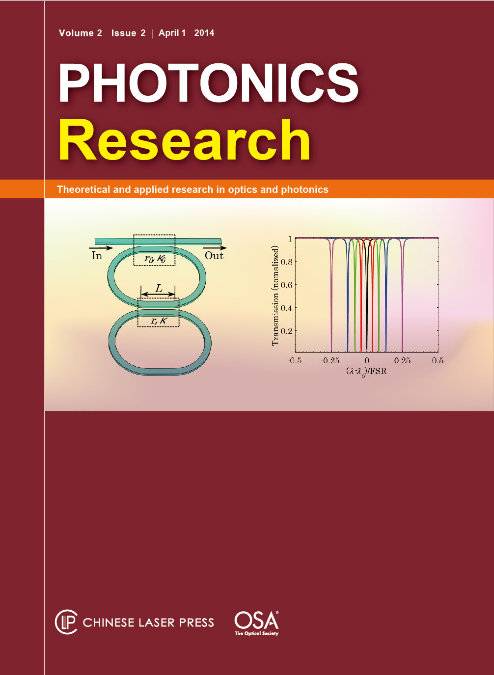
The proposed dual-ring structure is shown in Fig. 1(a). Both bus and ring waveguides have cross-sections of . Light inputs from bus waveguide and evanescently couples to the dual rings, while the coupling coefficient [15] is denoted with . The two rings have same shape, and the coupling coefficient between them is denoted with .
Fig. 1. Schematic of proposed structure. Inset, ridge waveguide cross-section view; BOX, buried oxide layer; , coupling length; , coupling coefficient; , self-coupling coefficient.
下载图片 查看所有图片
Based on coupled mode theory, the transmission () of this dual-ring structure can be expressed as where is the self-coupling coefficient, which is related to the coupling coefficient by () [16], and represents the transmission factor of one roundtrip of a single ring. is the roundtrip phase change of a single ring, expressed as , where is the roundtrip optical length and is the input wavelength.
According to Eq. (1), the transmission at different coupling coefficient () can be calculated, as shown in Fig. 2. At proper coupling strength, the transmission spectra of the dual-ring structure will split into two side peaks [17], as shown in Fig. 2(a). When coupling is enhanced (increasing ), the resonance splitting is intensified and the two side resonance peaks shift outwards. Figure 2(b) clearly depicts the resonance splitting with respect to . The two resonance peaks shift in opposite directions. Further analysis yields quantitative relations between resonance wavelength and coupling coefficient , as shown in Fig. 2(c). The two resonance peaks possess opposite signed and, within range of , is approximately constant, resulting in linear dependence between and .
Fig. 2. (a) Resonance splitting in dual-ring structure. (b) Resonance wavelength detuning at different ring-to-ring coupling coefficient. is the central wavelength, representing resonance wavelength at ; is the resonance wavelength; FSR stands for free spectral range. (c) with respect to coupling coefficient, approximately constant in a wide range of .
下载图片 查看所有图片
The coupling coefficient should be able to be adjusted in a wide range if resonance splitting is to be exploited for the athermal resonator. Racetrack microrings are capable of increasing ring-to-ring coupling, and are therefore adopted in our design as shown in Fig. 1(a). The coupling between the two rings is equivalent to a directional coupler (DC) with length . 3D full vector finite element method (FEM) is used to analyze this structure; the obtained energy flux is shown in Fig. 3(a) and field distribution is shown in Fig. 3(b). It is clearly shown that input light energy at upper waveguide alternately distributes in the two waveguides with increasing coupling length, in accordance with the coupled mode theory. Therefore by adjusting the length of DC, coupling coefficient will vary from to 1.
Fig. 3. Numerical analysis of (a) energy flux density () and (b) field distribution in DC.
下载图片 查看所有图片
Numerical analysis yields the relation of to coupling length , shown in Fig. 4(a). Simulation results (dots) are a sinusoidal function, in good agreement with the coupled mode theory (curves). For our symmetric DC structure, the analytical fit curve of is expressed as where is the coupling length of DC and is a constant determined by the cross-section of DC (waveguide width, height, and coupling gap).
Fig. 4. (a) Relations of coupling coefficient and (b) temperature sensitivity of coupling coefficient () versus coupling length at different temperature. Dots, simulation results; line, fitting curve based on coupled mode theory.
下载图片 查看所有图片
Moreover, varies with temperature. It can be explained that, when temperature increases, higher refractive index of silicon induces better confinement, hence weakening DC coupling ( decreases). The relations of are shown in Fig. 4(b), in which dots represent simulation results and curve fitting yields the expression In our design, the coupling gap of the DC is 100 nm, corresponding at , and .
According to the previous discussion, a positive or negative sign of can be acquired by choosing different resonance peaks, and can be controlled by DC coupling length. Hence, by optimizing the structure at an appropriate resonance wavelength, the blue shift caused by the resonance splitting can completely compensate the red shift caused by the TOC of the silicon material, resulting in athermal resonance and satisfying the equation where the induced by the TOC of silicon is a positive value, while is optimized to negative.
3. DEVICE PERFORMANCE
To illustrate the athermal working principles, we assume that the ring-to-ring coupling region (the DC gap with width of 100 nm) is immersed in negative TOC material of , which will magnify the . With the help of this magnification, we have designed an athermal microring with radius of 5 μm. To achieve zero coupling at , coupling length of DC can be set to , as illustrated in Fig. 4(a). Considering that the bent waveguide connected to the DC region also contributes to coupling, coupling length is optimized to be 21.2 μm (the total coupling is equivalent to 28 μm straight waveguide DC). Therefore, is satisfied at . The gap between the bus waveguide and first microring is optimized to 370 nm to reach critical coupling. The weak coupling, benefiting from such a large gap, is nearly independent of temperature variation.
3D full vector FEM simulated transmission spectra are shown in Fig. 5. When resonance splitting is not present (conventional microring), transmission spectra are shown in Fig. 5(a). It is clear that the resonator is not thermally stable and resonance wavelength shifts approximately . Figure 5(b) shows the transmission of the dual-ring structure with resonance splitting. When ambient temperature rises, resonance splitting increases accordingly. The left peak of the splitting is stabilized around 1550 nm, insensitive to temperature variation.
Fig. 5. Transmission spectra (a) without and (b) with resonance splitting.
下载图片 查看所有图片
Further, the presence of the other resonance mode (the right peak) will prohibit utilizing spectrum within two resonance modes for wavelength-division multiplexing (WDM); otherwise, crosstalk will happen. We note that the proposed athermal scheme occupies a relatively broad frequency spectrum in exchange for thermal stabilization. As shown in Fig. 5(b), realizing athermal operation within is at the cost of only one channel allowed in 1550–1554 nm wavelength, but the channel spacing may be reduced through optimal design. Also, other applications of this athermal scheme may not be limited by this phenomenon. Moreover, Fig. 5(b) shows that resonance peaks will be broader and extinction ratio will be smaller at higher temperature. The reason for this is that the structure is optimized to critical coupling at . When temperature increases, however, the device deviates from critical coupling condition due to variation of ring-to-ring coupling coefficient . In brief, variation of coupling causes degradation of linewidth and extinction ratio. For practical design, this degradation should also be taken into consideration.
Detailed analysis of resonance variation with temperature is shown in Fig. 6 (red line). It indicates that resonance wavelength variation is less than within 30 K temperature range, and variation increases with rising temperature. This can be explained by Eq. (4); the blue shift caused by resonance splitting can be expressed as shown in Fig. 6 (blue line). To obtain maximum athermal range, the working point of the proposed structure is set to at , and reaches its maximum, according to Eqs. (2) and (3). Blue shift decreases with rising temperature because, at increasing temperature, will rise and will drop, and nearly remains constant. Blue dots in Fig. 6 are numerical simulation results. Their accordance with the blue line fitted with Eq. (3) confirms the validity of the proposed athermal scheme based on dual-ring resonance splitting. It is worth noting that, although the proposed scheme and designed prototype is based on an all-pass microring, it can be easily extended to an add–drop microring since no modification is made on the microring itself in our scheme. Adding an additional waveguide under dual-ring will realize add-drop microring.
Fig. 6. Relations of blue shift (blue line and dots) and resonance wavelength shift (red line and crosses) versus temperature. is the resonance wavelength at , and is resonance wavelength.
下载图片 查看所有图片
4. CONCLUSION
This work proposes a novel athermal scheme utilizing resonance splitting of a dual-ring structure. Theoretic analysis and simulations are provided to prove its principles. An athermal resonator based on the proposed scheme is demonstrated, achieving lower than resonance wavelength variation within 30 K temperature range. This scheme uses resonance splitting, an intrinsic property of dual-ring structure, to compensate resonance red shift caused by TOC of silicon material and thus realize thermal stabilization. Therefore, further optimization in the ring-to-ring coupling region to enhance temperature sensitivity () is promising for applications in passive CMOS-compatible compact athermal SOI microrings, and pushing forward the development of on-chip, low-energy-consumption optoelectronic systems.
Qingzhong Deng, Xinbai Li, Zhiping Zhou, Huaxiang Yi. Athermal scheme based on resonance splitting for silicon-on-insulator microring resonators[J]. Photonics Research, 2014, 2(2): 02000071.
 Download: 824次


