Photonics Research, 2020, 8 (11): 11001734, Published Online: Oct. 28, 2020  

Nanowire-assisted microcavity in a photonic crystal waveguide and the enabled high-efficiency optical frequency conversions Download: 636次

Author Affiliations
1 Key Laboratory of Space Applied Physics and Chemistry, Ministry of Education, and Shaanxi Key Laboratory of Optical Information Technology, School of Physical Science and Technology, Northwestern Polytechnical University, Xi’an 710129, China
2 State Key Laboratory of Optoelectronic Materials & Technologies, School of Physics, Sun Yat-sen University, Guangzhou 510275, China
3 Department of Electronics and Nanoengineering, Aalto University, Espoo FI-00076, Finland
4 QTF Centre of Excellence, Department of Applied Physics, Aalto University, Espoo FI-00076, Finland
5 e-mail: jlzhao@nwpu.edu.cn
Abstract
We report an indium phosphide nanowire (NW)-induced cavity in a silicon planar photonic crystal (PPC) waveguide to improve the light–NW coupling. The integration of NW shifts the transmission band of the PPC waveguide into the mode gap of the bare waveguide, which gives rise to a microcavity located on the NW section. Resonant modes with Q factors exceeding 103 are obtained. Leveraging on the high density of the electric field in the microcavity, the light–NW interaction is enhanced strongly for efficient nonlinear frequency conversion. Second-harmonic generation and sum-frequency generation in the NW are realized with a continuous-wave pump laser in a power level of tens of microwatts, showing a cavity-enhancement factor of 112. The hybrid integration structure of NW-PPC waveguide and the self-formed microcavity not only opens a simple strategy to effectively enhance light–NW interactions, but also provides a compact platform to construct NW-based on-chip active devices.

1. INTRODUCTION

Semiconductor nanowires (NWs) have attracted intense research for constructing miniaturized nanophotonic and optoelectronic devices, including passive waveguides and resonators [13" target="_self" style="display: inline;">–3], and active light-emitting devices [46" target="_self" style="display: inline;">–6], photodetectors [7], and photovoltaic devices [8]. Unfortunately, the very poor couplings between NWs and light make it difficult to realize devices with high performance [9]. First of all, in contrast to a bulk material, the amount of substance in an NW is too small, which significantly limits the physical volume of light–matter interactions. Second, NWs’ diameters are in the scale of tens or hundreds of nanometers, which are smaller than the diffraction limit of an optical beam. With a further consideration of the much larger refractive indices of semiconductor NWs compared to the air, it is a challenge to launch light into NWs with an acceptable efficiency. To assist light–matter couplings in NWs, various photonic strategies have been utilized, including hybrid NWs with plasmonic structures [1013" target="_self" style="display: inline;">13], directly contacting NWs with microfiber for end couplings [14,15], and aligning NWs with on-chip waveguides and resonators [1619" target="_self" style="display: inline;">19]. Another viewpoint for future applications of NW devices is their integratability, which is very important in miniaturized and integrated systems. With those, it is intriguing to study integrations of NWs with on-chip photonic structures, which have no ohmic loss in the plasmonic structures and could provide more stable geometry than the couplings with microfibers. Especially for silicon and silicon nitride-based passive photonic chips, NW-integrations could supplement active functionalities of light sources, modulators, and detectors.

Planar photonic crystal (PPC) fabricated on dielectric slabs is well recognized as one of the important chip-integrated architectures. Leveraging their unique photonic structures, light–matter interactions and light wave propagations in PPC waveguides or cavities could be controlled effectively in a spatial scale of subwavelength, which is comparable to the thickness of NWs. Recently, a number of works have reported on the integration of NWs with PPC waveguides and nanocavities, which realize significantly enhanced light–NW couplings [18,2023" target="_self" style="display: inline;">23]. For instance, Notomi et al. demonstrated the first NW laser at the telecom band by integrating an InP NW into a groove trench of a silicon PPC waveguide, which induced a high-quality (Q) resonant mode [24]. In our previous work, high-efficiency second-harmonic generation (SHG) was achieved in an AlGaAs NW integrated on a PPC nanocavity, which could be pumped even by a continuous-wave (CW) laser with submicrowatt power [22].

In this article, we report efficiently enhanced light–NW couplings by integrating an InP NW onto a standard silicon PPC waveguide, as schematically shown in Figs. 1(a) and 1(b). Aligning the NW onto the PPC waveguide lowers the transmission bands of the waveguide with the perturbation of the mode refractive index. Several resonant modes with Q factors exceeding 103 are obtained relying on the mode gap, which are confirmed by numerically calculating the band diagrams of the NW-integrated and bare PPC waveguides. To illustrate that this architecture is good at improving light–matter couplings in NWs, we implement the cavity-assisted SHGs and sum-frequency generations (SFGs), as schematically shown in Fig. 1(c), which could be realized by a CW laser with a power of tens of microwatts. To the best of our knowledge, this is the first demonstration of SFG in NWs pumped by CW lasers. The demonstrated resonant modes in the hybrid NW–PPC waveguide are governed by the mode gap in the photonic bandgap and dispersion of the waveguide mode, length of the NW, and position of the NW. This result indicates the possibility of inducing cavities by integrating an NW onto a standard PPC waveguide, which has no requirement of extra complicated lithography and etching steps for forming a groove trench [20,24]. It promises a simple and reliable route to realizing reconfigurable and tunable cavities in PPC waveguides in the postprocessing of chip-integrated devices.
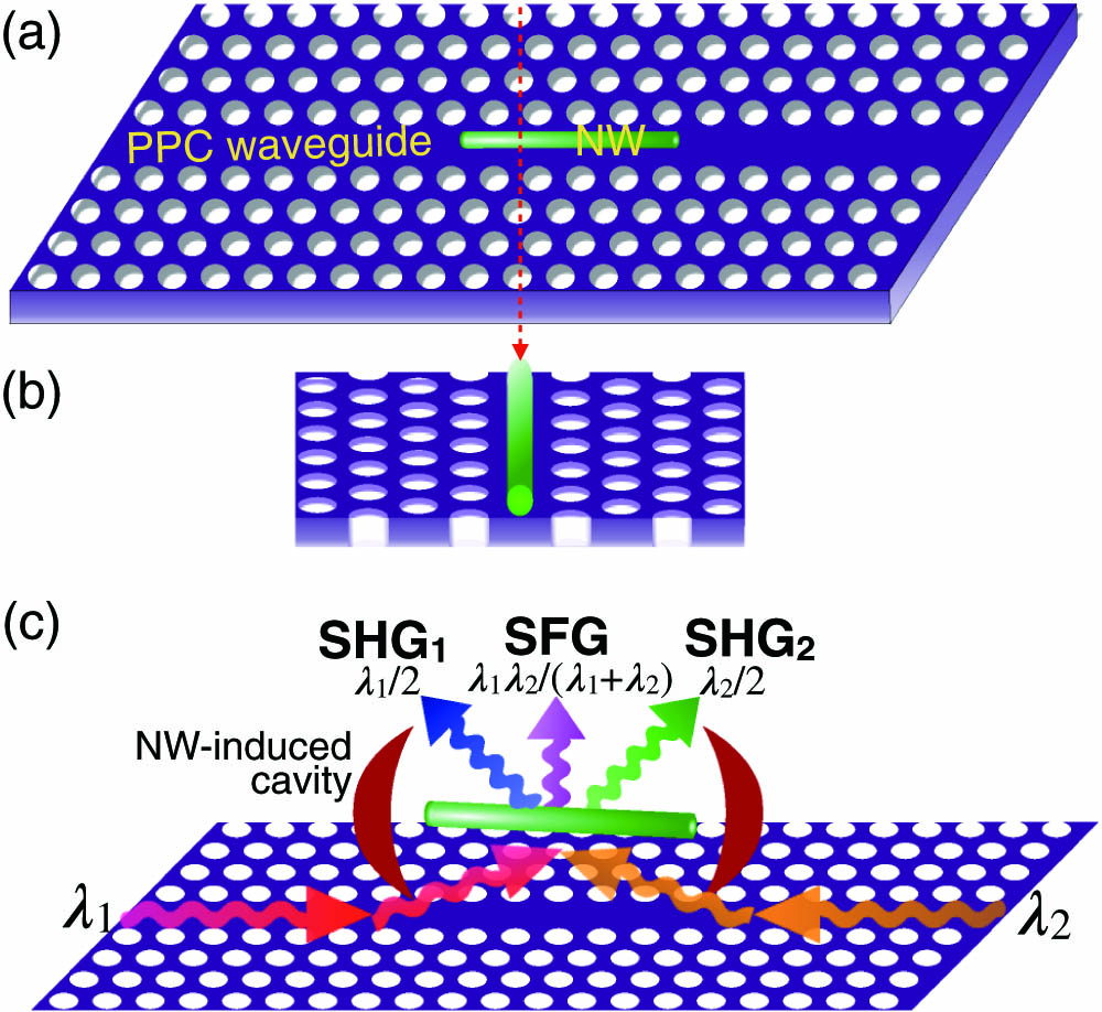
Fig. 1. (a), (b) Schematic representations of the hybrid structure of an NW and a PPC waveguide; (c) operation principle of the optical frequency upconversion processes (SHG and SFG) with the enhanced light–NW coupling by the NW-induced cavity.

下载图片 查看所有图片

2. HYBRID STRUCTURE OF THE NW AND PPC WAVEGUIDE

The employed PPC waveguide is formed by missing a line of air holes in a triangle-lattice PPC slab. The PPC lattice constant is a=420  nm and the air-hole radius is r=120  nm. The two nearest neighbor air-hole rows surrounding the waveguide are moved away from the line defect by 60 nm. Note this shift of air holes is not necessary in forming cavities in the hybrid NW–PPC waveguide, which is confirmed by further simulations. The PPC waveguide is fabricated in a silicon-on-insulator substrate with a 220 nm thick top silicon slab with the combinations of electron beam lithography and inductively coupled plasmon etching. After those, wet etching is employed to undercut the bottom silicon oxide layer to realize an air-suspended PPC waveguide. To facilitate the light coupling of the PPC waveguide, it is connected by silicon ridge waveguides at the two ends, which are then terminated by inverse tapers and embedded in polymer butt couplers to provide a coupling loss of 5 dB with an optical-lensed fiber [25].

To integrate the InP NW onto the PPC waveguide, a single NW is picked up from the vertically grown NW cluster using a tungsten probe, which is grown on a silicon substrate in a horizontal flow atmospheric pressure metal–organic vapor phase epitaxy system [26]. With the assistance of a high-resolution motorized stage, the NW is dropped onto the pattern of the PPC waveguide from the tungsten probe. To further align the NW with the line defect of the PPC waveguide, an atomic force microscope (AFM)-assisted manipulation technique is exploited. The location of the NW with respect to the PPC waveguide is examined first with a full AFM image. Then the NW is pushed accordingly to align onto the line defect using the AFM probe. Figure 2(a) displays the scanning electron microscope (SEM) image of the finished device, showing an NW locating at the center of the line defect. The lower side of the NW is parallel to the defect line, implying the feasibility of the integration technique based on the AFM manipulation. Unfortunately, the NW has a tapered structure due to the sidewall growth in the metal-catalyzing epitaxy process. Its upper side cannot be parallel to the line defect anymore. In the future, NWs grown by the selective-area epitaxy technique could be chosen to ensure a uniform diameter along the NW growth direction [27]. Estimated from the SEM image, the diameters of the NW’s two ends are about 220 and 160 nm, respectively, and the NW length is about 7.12 μm.

Fig. 2. (a) SEM image of the fabricated device, showing the precise alignment of the NW with the line defect of the PPC waveguide; (b) normalized transmission spectra of the PPC waveguide before and after the integration of the NW, where the asterisks indicate the locations of the resonance modes of the NW-induced PPC cavity; (c) transmission spectra around the resonant mode at 1509 nm when the input laser has different powers of 5 mW (blue dots), 10 mW (red dots), and 15 mW (green dots). Black lines are fitting curves with Fano-type line shapes.

下载图片 查看所有图片

To characterize the perturbation of the NW on the transmission properties of the PPC waveguide, transmission spectra of the PPC waveguide before and after the integration of the NW are measured, as shown in Fig. 2(b). A narrowband CW tunable laser is incident onto one of the polymer butt couplers as the light source. With the laser wavelength tuned from 1500 to 1600 nm by a step of 0.01 nm, transmission spectra of the PPC waveguide are obtained by measuring the optical powers output from the polymer butt coupler at the other end. The laser power is maintained at 10 mW during the wavelength scanning.

From the bare PPC waveguide, a transmission band in the wavelength range between 1515 and 1560 nm is obtained. After the integration of the NW, the transmission spectrum is subject to significant modifications, indicating the effective coupling between the NW and the PPC waveguide. The transmission band presented in the bare PPC waveguide becomes a transmission valley, and two broad peaks are observed around the wavelengths of 1506 and 1565 nm, which have several transmission dips. These features could be explained by the formations of microcavities on the hybrid NW–waveguide relying on the Fabry–Perot (FP) oscillations and the photonic bandgap of the PPC [20,28,31].

As shown in Fig. 2(a), the NW covers part of the PPC waveguide. Its integration would induce a positive perturbation of the dielectric function over this waveguide region. The effective refractive index of the guiding mode in this NW-covered region is larger than that in the bare waveguide regions on the two sides. It consequently forms an FP-type cavity, with the two ends of the NW-covered region as two mirrors. There are therefore resonant peaks centering around the wavelengths of 1506 and 1565 nm in the transmission spectrum. The wavelength difference between them could be considered as the free spectral range (FSR) of the FP cavity, which is determined by FSR=λ02/(2neffL). Here, L=7.12  μm is the cavity length, and the central resonance wavelength is λ0=1506  nm. With the measured FSR of 59 nm, the effective refractive index of the guiding mode in the silicon PPC waveguide neff is estimated as 2.7, which is close to the numerically calculated effective refractive index of 2.65. Because of the small index contrast between NW-covered and bare waveguide regions, reflectances of the two mirrors are low, which results in the broad linewidths of the resonant peaks, i.e., low Q factors of the resonance modes. In addition, since the main transmission band (1515–1560 nm) of the bare PPC waveguide locates at the off-resonance region of the FP cavity, the transmission becomes a valley in this wavelength region after the NW integration, as shown in Fig. 2(b). The locations of the two FP resonant peaks at the opposite sides of the transmission band of the bare PPC waveguide are determined by the constructive interference of the standing waves. If the length, diameter, and location of the NW are changed, the FP resonant peaks are expected to shift to other wavelength ranges, such as locating at the central region of the transmission band of the bare PPC waveguide.

Besides the FP cavity formed by the optical reflections at the two ends of the NW-covered waveguide region, the NW also perturbs the dispersion band of the guiding mode in the PPC waveguide to have lower optical frequencies, as discussed in Fig. 3(a). It gives rise to a mode gap between the modes guided in the NW-covered and bare PPC waveguides. This allows the light to be confined in the NW-covered region, and the bare PPC waveguides on the two sides to act as barriers [20,28]. Consequently, resonant modes are formed, leveraging the photonic band structure of the PPC, which are expected to have high Q factors [29,30]. We recognize this cavity as a type of PPC cavity. Since it spatially overlaps with the above-mentioned FP cavity, their resonant modes are coupled with each other [31]. Resonant modes of the PPC cavity present narrowband transmission dips over the broadband resonant peaks of the FP cavity, as shown in Fig. 2(b). Also, because of the gradually varied phase over the broad resonant peak of the FP cavity, these transmission dips show asymmetric Fano-type line shapes with varied asymmetric slopes and signs [31]. From the locations of the transmission dips, resonant modes of the PPC cavity are distinguished. By fitting these transmission dips with Fano-type line shapes, the central resonant wavelengths are recognized at 1504.2, 1509.0, 1552.0, 1554.8, and 1557.2 nm, and the corresponding Q factors are estimated as 2500, 1700, 1500, 3100, and 1700, respectively. In this fabricated sample, the NW is not perfectly aligned at the center of the PPC waveguide. As discussed in our previous work [23], which studied the mode coupling between an NW and a PPC nanocavity, both the Q factors and the resonant wavelengths of the resonant modes are expected to be changed as the NW is gradually moved away from the center of the PPC waveguide. These variations could be attributed to the modified coupling strengths between the NW and the optical mode, which is determined by the mode distributions of the PPC waveguide. In future work, the optimized location of the NW on the PPC waveguide for maximum Q factor and specific resonant wavelength could be studied by moving the NW carefully, as demonstrated in Ref. [23].

Fig. 3. (a) Band diagram of the odd (upper) and even (lower) guiding modes in the PPC waveguides with (red square) and without (black square) the NW; (b) mode distributions of the even and odd resonant modes at different orders calculated from an NW-integrated PPC waveguide. The arrows indicate that the resonant modes arise from the localizations of the corresponding odd and even transmission bands of the NW-integrated PPC waveguide.

下载图片 查看所有图片

Resonance properties of the above-obtained modes at the transmission dips are further verified by silicon’s thermal-optic effect. Because of the two-photon absorption effect, a telecom band light with a high power transmitted through silicon would yield thermal heating, which modifies silicon’s refractive index via the thermal-optic effect. For the NW-induced resonant modes on the PPC waveguide, relying on the high Q factors, the incident on-resonance light could heat the cavity effectively, and the resonant wavelength would be redshifted subsequently due to the increased refractive index. Figure 2(c) displays the transmission spectra of the NW–PPC waveguide around the resonant mode of 1509.0 nm when the laser power is set as 5, 10, and 15 mW. The transmission dips are fitted using Fano-type line shapes, as shown by the black curves. The fitting results indicate the Q factor of the resonant mode maintains at 1700 for different pump powers. However, the central wavelength of the transmission dip locates at 1508.9, 1509.0, and 1509.1 nm, respectively, when the laser power is set as 5, 10, and 15 mW. This redshift of the resonant wavelength with a rate of 0.02 nm/mW verifies the resonant properties of the cavity.

3. SIMULATION OF THE RESONANT MODES

To further reveal the formation mechanisms of the NW-induced cavities, we carry out the simulations of the dispersion diagram for the transverse electric (TE) modes of PPC waveguides with and without NWs separately, as shown in Fig. 3(a). Here, the structure parameters of the PPC waveguide employed in the experiment are utilized, and the refractive indices of the silicon and the InP NW are chosen as 3.47 and 3.16, respectively. The diameter and length of the NW are set as 200 nm and 7.12 μm. Modes are plotted as a function of the in-plane crystal momentum kx (in units of 2π/a) and mode frequency (in units of a/λ), and the dashed blue line represents the light line of the PPC slab. The well-recognized odd (upper) and even (lower) transmission bands of the PPC waveguide are both shifted downward to lower frequencies by the integration of the NW [20,28]. Part of the guiding modes in the NW-integrated waveguide shift into the mode gap of the bare PPC waveguide. As a result, for the fabricated device with an NW covered on part of the PPC waveguide, it is possible to realize localized guiding modes in the NW-covered region due to the forbidden propagation in the bare waveguide sections on the two sides.

To confirm that, we numerically solve the resonant modes of the fabricated device using a finite-element technique. The distributions of the x (Ex) and y (Ey) components of the modes’ electric fields are displayed in Fig. 3(b). The resonant modes have the same field distributions and symmetries as the guiding modes in the even and odd transmission bands of the NW-integrated PPC waveguide. Accordingly, we recognize them as “even mode” and “odd mode,” respectively. Here, we only show the three lowest order resonant modes from each transmission band. The resonant wavelengths for the first to third odd modes are 1482.5, 1477.9, and 1471.8 nm, respectively, which are consistent with the mode-gap region located by the odd transmission band of the NW-integrated PPC waveguide. The resonant wavelengths for the first to third even modes are 1557.4, 1555.2, and 1553.3 nm, respectively, located in the even transmission band of the NW-integrated PPC waveguide. The correspondences between the transmission bands and the resonant modes are indicated by the arrows in Fig. 3. Those resonant modes have Q factors in the order of 104. In addition, with the reflections from the bare waveguide sections on the two sides, the resonant modes in the central NW-covered section are formed by the standing-wave condition. Hence, resonant modes with different orders have varied wave packets. The field distributions also indicate the electric field penetrates into the NW effectively for the Ex components, which promises the effective light–NW couplings. However, for the Ey component, there is no electric field in the NW due to the depolarization effect governed by the NW’s high refractive index and the subwavelength diameter [32,33].

Comparing these simulation results with the above experiment results, though their resonant wavelengths cannot match correspondingly, the even and odd resonant modes separated by a large wavelength range (about 50 nm) are observed experimentally. And the FSR for the even (odd) resonant modes obtained in the experiments are similar as those calculated in the simulated resonant modes. In the simulation, the FSRs for the even resonant modes are 2.2 and 1.9 nm, which are 2.4 and 2.8 nm in the experiment, respectively. For the odd resonant modes, the FSRs are 4.6 and 4.8 nm obtained in the simulation and experiment, respectively. Determined by the dispersion properties of the even and odd transmission bands of the NW-integrated PPC waveguide, the FSR of the even resonant modes has a smaller wavelength difference than that of the odd resonant modes.

4. EXPERIMENTAL RESULTS OF SHG AND SFG

To illustrate the effectively enhanced light–NW coupling in the NW–PPC waveguide, we then test different optical frequency upconversion processes in the hybrid structure, including SHGs and SFGs. In III–V compound semiconductor NWs, such as InP and GaAs, second-order nonlinear optical properties are allowed due to the absence of central inversion symmetry in the crystal structure. Optical frequency upconversion (SHGs and SFGs) and downconversion processes enabled by NWs’ second-order nonlinearity are intriguing for nonlinear optical nanoscopy [34,35], nanoscale light sources [9], and optical autocorrelators [15]. However, limited by the weak light–matter coupling [36], most of the previous studies about SHGs in NWs have to be implemented using pulsed lasers with high peak powers (>100  W), hindering their device applications. Also, because of the essential pump with pulsed lasers, SFGs in NWs were seldom reported, which require precise and complex synchronization of two laser pulses.

Here, in the fabricated hybrid NW–PPC waveguide, high-efficiency SHGs and SFGs are realized with pumps of CW lasers in the power levels of tens of microwatts. It is the result of the effective light–NW couplings enabled by NW-induced resonant modes on the PPC waveguide. The on-resonance light would circulate in the NW for a long time τ (τ=Q/ω; ω is the resonant frequency). In addition, as demonstrated in the above mode simulations, the mode field largely overlaps with the NW. In the experiments, CW narrowband lasers with tunable wavelengths are utilized to excite the frequency upconversion signals, which are tuned to be on-resonance with the resonant modes induced by the NW. Since the resonant modes are in the telecom band, the enhanced SHG and SFG signals are expected to be in the wavelength range between 750 and 800 nm. It is impossible to examine them from their direct transmissions along the PPC waveguide considering silicon’s strong optical absorption. We therefore monitor them by collecting the vertical scattering signals from the NW region using a home-built vertical microscope with an objective lens (20×, with a numerical aperture of 0.42). The pump lasers are scattered by the NW as well, which would be filtered out by a short-pass dichroic mirror. The finally left frequency upconversion signals are examined by a spectrometer mounted with a cooled silicon camera.

With a CW laser at the wavelength of 1509.0 nm (wavelength of one of the NW-induced resonance modes) coupled into the hybrid NW–PPC waveguide, the acquired spectrum of the scattered frequency upconversion signal is shown in Fig. 4(a). A strong peak is observed at the wavelength of 754.5 nm, corresponding to the half-wavelength of the pump laser. To illustrate this peak arising from the SHG process, we examine its power dependence on the pump power, which varies from 0.5 to 15 mW. Figure 4(b) plots a relation between the pump powers and SHG powers in a log-log scale, which is fitted by a line with a slope of 2.08. The obtained SHG powers represent a quadratic function of the pump powers, which is governed by a process wherein two photons of the fundamental wave convert into one photon of the SHG wave. Considering the coupling loss (5  dB) from the lensed fiber to the input coupler and the transmission loss (>5  dB) of the PPC waveguide, the pump power accessing the NW-covered waveguide section is no more than 10% of the incident laser power. Considerable SHG signals could be observed even when the laser power is as low as 0.5 mW. Hence, with tens of microwatts of a CW laser pumped on the NW-integrated PPC waveguide, SHG could be achieved, which is in contrast to the previously reported NW SHG pumped by pulsed lasers. It indicates the high-efficiency second-order nonlinear process enabled by the NW-induced cavity on the PPC waveguide.

Fig. 4. (a) Spectrum of SHG from the vertical scattering signal of the NW–PPC waveguide with the pump of a 1509.0 nm laser; (b) log-log plot of the SHG powers and pump powers fitted by a line with a slope of 2.08; (c) measured SHG powers when the pump laser is scanned over the wavelength range of 1500–1600 nm, where the linear transmission spectrum of the pump laser is shown as well for cross-reference; (d) polarization property of the scattered SHG signal, where the polar angle is defined with respect to the long axis of the NW.

下载图片 查看所有图片

To further verify the resonantly enhanced SHG, the wavelength of the CW laser is scanned from 1500 to 1600 nm, and the corresponding scattered SHG signals are recorded, as shown by the blue curve in Fig. 4(c). To assist the comparison, the linear transmission spectrum of the laser is also displayed in the red curve. Only when the laser is tuned on-resonance with the NW-induced resonant modes, could the strong SHG signals be detected. By comparing the SHG powers obtained with the pump laser on-resonance with the mode at 1509.0 nm and off-resonance, an enhancement factor of 112 is estimated. This illustrates the effectively enhanced light–NW coupling in the NW-induced PPC cavity. Note the measured SHG powers generated by other on-resonance pumps are much lower than those pumped by the 1509.0 nm laser. We attribute it to the specific scattering spots and directions of the NW’s SHG signals pumped by different resonant modes, which are determined by the tensor of the second-order nonlinear coefficient (χ(2)) of the NW and near fields of the resonant modes. In the experiments, we could boost the collected powers of the SHG signals pumped by any one of the resonant modes by moving the device slightly in-plane with respect to the objective lens.

In previous works about NW SHGs, the measurements were carried out in a configuration with normal illumination and normal collection. Dependences of NW SHGs on the laser polarizations and the signal collection polarizations are normally studied, which facilitates the understandings of light–NW interactions and NW crystal structures [37,38]. In this NW-PPC waveguide experiment, the pump laser is side-launched from the PPC waveguide, which then excites the NW SHG via the evanescent field of the NW-induced resonant modes. Hence, the light–NW interaction is governed by the near field of the resonant mode, which would not be modified by the polarization direction of the pump laser. The laser polarization only changes its coupling efficiency to the guiding mode of the PPC waveguide. We therefore only study the polarization properties of the scattered SHG signal from the NW–PPC waveguide by placing a polarizer in the signal collection path. The varied intensities of the scattered SHG signal polarized along different directions are monitored using the spectrometer. Note the employed grating of the monochromator (Princeton Instruments SP-2558, with a grating of 150 G/mm at 800 nm) has almost no difference for the s- and p-polarized light at the wavelength around 750 nm. The results acquired from the spectrometer could reveal the real polarization properties of the scattered SHG signal. The measured result is displayed in Fig. 4(d), where the polar angle θ is defined as the angle between the polarizer and NW’s long axis. The scattered SHGs have strong anisotropy along different polarizations, and the maximum SHG is not collected from the component polarized along the long axis of the NW, but with a small angle.

This polarization property could be explained well by the depolarization effect of the electric field inside the NW [32,33]. Under the quasi-static approximation, because the NW diameter is smaller than the SHG wavelength and there is a large refractive index difference between NW and air, the electric field perpendicular to the long axis of the NW will be attenuated by a factor of 2/(1+nNW2)=0.153. Here, nNW is the refractive index of the InP NW, which is about 3.47 around the SHG wavelength. The SHG radiation could be simply regarded as dipole radiations driven by second-order nonlinear polarizations (P2ω) oscillating at the frequency of SHG (2ω). The component of P2ω perpendicular to the NW’s long axis is reduced by a factor of 0.153. The SHG signal radiated by this component polarizes perpendicularly to the NW’s long axis, and the power is attenuated by a factor of 0.0234. In contrast, the parallel component of P2ω is not modified by the depolarization effect because the NW length is much larger than the optical wavelength. The SHG radiated by this component is not reduced either, which polarizes along the NW’s long axis. We defined the collected SHG powers polarized parallel and perpendicularly to the NW’s long axis as P and P. The theoretical anisotropic ratio (PP)/(P+P) is calculated as 0.954. Estimated from the experimental data, the anisotropic ratio is about 0.934, which is consistent with the theoretical calculation. The fitting curve in Fig. 4(d) has a function of (cosθ+0.153sinθ)2, which agrees well with the experiment data.

The successful excitation of SHG with a low-power CW laser in the NW–PPC waveguide indicates it is convenient to implement other second-order nonlinear processes leveraging the exemption of synchronization of multiple pulsed lasers [39]. To carry that out, we employ two CW tunable narrowband lasers (Laser1 and Laser2) simultaneously as the pumps, which are incident onto the PPC waveguide via the two end couplers separately, as schematically shown in Fig. 1(c). Their wavelengths are first tuned as 1509.0 nm (Laser1) and 1554.8 nm (Laser2) to resonantly excite the two resonant modes. By setting the powers of the two CW pumps as 1 mW, the generated frequency upconversion signals collected from the NW present a spectrum shown in Fig. 5(a). Three peaks at the wavelengths of 754.5, 765.8, and 777.4 nm are observed. According to the wavelength conversion, they are recognized as the SHGs and SFG of the two pump lasers, which are labeled as SHG1, SFG, and SHG2 successively in Fig. 5(a). Pump power dependence of the SFG is studied by changing the powers of the two lasers simultaneously with the same values. Figure 5(b) plots the measurement result in the log-log scale. In the process of SFG, both Laser1 and Laser2 are involved. The generation of one SFG photon requires the contributions of one photon from Laser1 and one photon from Laser2. Hence, when the powers of both lasers vary simultaneously, the SFG powers should be a quadratic function of the pump powers, which is consistent with the fitting slope of 2.03 in Fig. 5(b).

Fig. 5. (a) Spectrum of the scattered frequency upconversion signals pumped by two on-resonance lasers at 1509.0 and 1554.8 nm, showing SHG and SFG signals; (b) log-log plot of the SFG powers and pump powers fitted by a line with a slope of 2.03; (c) measured SFG powers with one pump laser fixed at 1509.0 nm and the other pump laser scanned across 1540–1570 nm, where the linear transmission spectrum of the pump laser is shown as well for cross-reference; (d) polarization properties of SHG and SFG signals with respect to the long axis of the NW.

下载图片 查看所有图片

The possibility of SFG pumped by two low-power CW lasers is the result of the effective light–NW coupling endowed by the NW-induced resonant modes at 1509.0 and 1554.8 nm. It could be proved by examining the dependence of the SFG on the pump wavelength. We fix the wavelength of Laser1 (1509.0 nm), and scan the wavelength of Laser2 over a range between 1540 and 1570 nm. The SFG powers are recorded for each wavelength of Laser2, as shown by the blue curve of Fig. 5(c). The linear transmission spectrum of the NW–PPC waveguide over this wavelength range is shown as well for comparison. When the wavelength of Laser2 is tuned as 1552.0, 1554.8, and 1557.2 nm, which are wavelengths of the resonant modes, there are peaks of SFG powers. As the laser wavelength is detuned away from these resonant modes, the SFG signal decreases to undetectable levels. SFG is governed by the two pump lasers. If there is no resonant mode enhancing the interaction between the NW and Laser2, the SFG cannot be achieved effectively, though the SHG1 signal is maintained all the time because the Laser1 is on-resonantly pumping the resonant mode at 1509.0 nm. Note that there is a weak SFG peak when the Laser2 has a wavelength of 1549.5 nm. It might be another resonant mode of the NW-induced cavity. The absence of dip in the transmission spectrum is caused by the weak coupling between the resonant mode and the guiding mode of PPC waveguide. The polarization properties of SHG1, SFG, and SHG2 are characterized, as shown in Fig. 5(c). Governed by the depolarization effect along the direction perpendicular to the long axis of the NW, the far-field scattered frequency upconversion signals have anisotropic polarizations. All of them could be fitted by the function of (cosθ+0.153sinθ)2 well.

5. CONCLUSIONS

In conclusion, by integrating an InP NW onto a silicon PPC waveguide, effective light–NW interactions are realized by forming resonant modes with Q factors exceeding 103, which are illustrated by the NW’s effective SHGs and SFGs pumped by CW lasers in the power levels of tens of microwatts. Combined with the calculations of the band diagram of the PPC waveguide with and without NW, the formed cavities are attributed to the lowered transmission band by the NW integration. By comparing the SHG signals pumped with on-resonance and off-resonance lasers, a cavity enhancement factor of 112 is obtained, indicating the strongly enhanced light–NW coupling in the NW-induced PPC cavity. The effective light–NW couplings in the hybrid NW-PPC waveguide not only provide a strategy to design on-chip microcavities with the possibility of postprocessing, but also present the potential to expand functionalities on silicon or silicon nitride chips with the assistance of NW’s active attributes, such as lasers, photodetectors, and modulators. While the adapted AFM manipulation technique has low yield for NW integration, there are two possible strategies for large-scale NW-integrated photonic devices based on the well-developed nanofabrication and NW growth techniques. (1) NWs are first grown on silicon or silicon nitride wafers, which are used for fabricating a PPC waveguide. The hybrid structures are then realized by designing and fabricating the PPC waveguides around the pre-growth NWs. (2) On the pre-fabricated silicon or silicon nitride PPC waveguide, the NWs are grown precisely in situ on the patterns using the selective-area growth technique [40].

References

[1] A. Fu, H. Gao, P. Petrov, P. Yang. Widely tunable distributed Bragg reflectors integrated into nanowire waveguides. Nano Lett., 2015, 15: 6909-6913.

[2] R. Yan, D. Gargas, P. Yang. Nanowire photonics. Nat. Photonics, 2009, 3: 569-576.

[3] X. Guo, Y. Ying, L. Tong. Photonic nanowires: from subwavelength waveguides to optical sensors. Acc. Chem. Res., 2014, 47: 656-666.

[4] S. W. Eaton, A. Fu, A. B. Wong, C. Z. Ning, P. Yang. Semiconductor nanowire lasers. Nat. Rev. Mater., 2016, 1: 16028.

[5] J. Sun, M. Han, Y. Gu, Z. X. Yang, H. Zeng. Recent advances in group III–V nanowire infrared detectors. Adv. Opt. Mater., 2018, 6: 1800256.

[6] W. Luo, Q. Weng, M. Long, P. Wang, F. Gong, H. Fang, M. Luo, W. Wang, Z. Wang, D. Zheng, W. Hu, X. Chen, W. Lu. Room-temperature single-photon detector based on single nanowire. Nano Lett., 2018, 18: 5439-5445.

[7] L. Hu, Q. Liao, Z. Xu, J. Yuan, Y. Ke, Y. Zhang, W. Zhang, G. P. Wang, S. Ruan, Y. J. Zeng, S. T. Han. Defect reconstruction triggered full-color photodetection in single nanowire phototransistor. ACS Photon., 2019, 6: 886-894.

[8] E. Garnett, P. Yang. Light trapping in silicon nanowire solar cells. Nano Lett., 2010, 10: 1082-1087.

[9] C.-Z. Ning. Semiconductor nanolasers and the size-energy-efficiency challenge: a review. Adv. Photon., 2019, 1: 014002.

[10] X. Liu, Q. Zhang, J. N. Yip, Q. Xiong, T. C. Sum. Wavelength tunable single nanowire lasers based on surface plasmon polariton enhanced Burstein-Moss effect. Nano Lett., 2013, 13: 5336-5343.

[11] Y. S. No, J. H. Choi, H. S. Ee, M. S. Hwang, K. Y. Jeong, E. K. Lee, M. K. Seo, S. H. Kwon, H. G. Park. A double-strip plasmonic waveguide coupled to an electrically driven nanowire LED. Nano Letters, 2013, 13: 772-776.

[12] C.-H. Cho, C. O. Aspetti, M. E. Turk, J. M. Kikkawa, S.-W. Nam, R. Agarwal. Tailoring hot-exciton emission and lifetimes in semiconducting nanowires via whispering-gallery nanocavity plasmons. Nat. Mater., 2011, 10: 669-675.

[13] J. Ho, J. Tatebayashi, S. Sergent, C. F. Fong, S. Iwamoto, Y. Arakawa. Low-threshold near-infrared GaAs-AlGaAs core-shell nanowire plasmon laser. ACS Photon., 2015, 2: 165-171.

[14] J. Zhou, F. Gu, X. Liu, J. Qiu. Enhanced multiphoton upconversion in single nanowires by waveguiding excitation. Adv. Opt. Mater., 2016, 4: 1174-1178.

[15] C. Xin, S. Yu, Q. Bao, X. Wu, B. Chen, Y. Wang, Y. Xu, Z. Yang, L. Tong. Single CdTe nanowire optical correlator for femtojoule pulses. Nano Lett., 2016, 16: 4807-4810.

[16] B. Chen, H. Wu, C. Xin, D. Dai, L. Tong. Flexible integration of free-standing nanowires into silicon photonics. Nat. Commun., 2017, 8: 20.

[17] J. Xie, X. Hu, C. Li, F. Wang, P. Xu, L. Tong, H. Yang, Q. Gong. On-chip dual electro-optic and optoelectric modulation based on ZnO nanowire-coated photonic crystal nanocavity. Adv. Opt. Mater., 2018, 6: 1800374.

[18] C. E. Wilhelm, M. I. B. Utama, G. Lehoucq, Q. Xiong, C. Soci, D. Dolfi, A. De Rossi, S. Combrie. Broadband tunable hybrid photonic crystal-nanowire light emitter. IEEE J. Sel. Top. Quantum Electron., 2017, 23: 2736602.

[19] H. G. Park, C. J. Barrelet, Y. Wu, B. Tian, F. Qian, C. M. Lieber. A wavelength-selective photonic-crystal waveguide coupled to a nanowire light source. Nat. Photonics, 2008, 2: 622-626.

[20] M. D. Birowosuto, A. Yokoo, G. Zhang, K. Tateno, E. Kuramochi, H. Taniyama, M. Takiguchi, M. Notomi. Movable high-Q nanoresonators realized by semiconductor nanowires on a Si photonic crystal platform. Nat. Mater., 2014, 13: 279-285.

[21] M. Takiguchi, A. Yokoo, K. Nozaki, M. D. Birowosuto, K. Tateno, G. Zhang, E. Kuramochi, A. Shinya, M. Notomi. Continuous-wave operation and 10-Gb/s direct modulation of InAsP/InP sub-wavelength nanowire laser on silicon photonic crystal. APL Photon., 2017, 2: 046106.

[22] Q. Yuan, L. Fang, H. Yang, X. Gan, V. Khayrudinov, H. Lipsanen, Z. Sun, J. Zhao. Low-power continuous-wave second harmonic generation in semiconductor nanowires. Laser Photon. Rev., 2018, 12: 1800126.

[23] Q. Yuan, L. Fang, Y. Wang, B. Mao, J. Zhao, X. Gan, Q. Zhao, V. Khayrudinov, H. Lipsanen, Z. Sun. Mode couplings of a semiconductor nanowire scanning across a photonic crystal nanocavity. Chin. Opt. Lett., 2019, 17: 062301.

[24] A. Yokoo, M. Takiguchi, M. D. Birowosuto, K. Tateno, G. Zhang, E. Kuramochi, A. Shinya, H. Taniyama, M. Notomi. Subwavelength nanowire lasers on a silicon photonic crystal operating at telecom wavelengths. ACS Photon., 2017, 4: 355-362.

[25] C. Monat, C. Grillet, M. Collins, A. Clark, J. Schroeder, C. Xiong, J. Li, L. O’Faolain, T. F. Krauss, B. J. Eggleton, D. J. Moss. Integrated optical auto-correlator based on third-harmonic generation in a silicon photonic crystal waveguide. Nat. Commun., 2014, 5: 3246.

[26] Q. Gao, V. G. Dubrovskii, P. Caroff, J. Wong-Leung, L. Li, Y. Guo, L. Fu, H. H. Tan, C. Jagadish. Simultaneous selective-area and vapor-liquid-solid growth of InP nanowire arrays. Nano Lett., 2016, 16: 4361-4367.

[27] Q. Gao, D. Saxena, F. Wang, L. Fu, S. Mokkapati, Y. Guo, L. Li, J. Wong-Leung, P. Caroff, H. H. Tan, C. Jagadish. Selective-area epitaxy of pure wurtzite InP nanowires: high quantum efficiency and room-temperature lasing. Nano Lett., 2014, 14: 5206-5211.

[28] B. S. Song, S. Noda, T. Asano, Y. Akahane. Ultra-high-Q photonic double-heterostructure nanocavity. Nat. Mater., 2005, 4: 207-210.

[29] A. A. Bogdanov, K. L. Koshelev, P. V. Kapitanova, M. V. Rybin, S. A. Gladyshev, Z. F. Sadrieva, K. B. Samusev, Y. S. Kivshar, M. F. Limonov. Bound states in the continuum and Fano resonances in the strong mode coupling regime. Adv. Photon., 2019, 1: 016001.

[30] B. Qiang, A. M. Dubrovkin, H. N. S. Krishnamoorthy, Q. Wang, C. Soci, Y. Zhang, J. Teng, Q. J. Wang. High Q-factor controllable phononic modes in hybrid phononic-dielectric structures. Adv. Photon., 2019, 1: 026001.

[31] L. Gu, H. Fang, J. Li, L. Fang, S. J. Chua, J. Zhao, X. Gan. A compact structure for realizing Lorentzian, Fano, and electromagnetically induced transparency resonance lineshapes in a microring resonator. Nanophotonics, 2019, 8: 841-848.

[32] J. P. Long, B. S. Simpkins, D. J. Rowenhorst, P. E. Pehrsson. Far-field imaging of optical second-harmonic generation in single GaN nanowires. Nano Lett., 2007, 7: 831-836.

[33] J. Wang, M. S. Gudiksen, X. Duan, Y. Cui, C. M. Lieber. Highly polarized photoluminescence and photodetection from single indium phosphide nanowires. Science, 2001, 293: 1455-1457.

[34] Y. Nakayama, P. J. Pauzauskie, A. Radenovic, R. M. Onorato, R. J. Saykally, J. Liphardt, P. Yang. Tunable nanowire nonlinear optical probe. Nature, 2007, 447: 1098-1101.

[35] B. Sain, C. Meier, T. Zentgraf. Nonlinear optics in all-dielectric nanoantennas and metasurfaces: a review. Adv. Photon., 2019, 1: 024002.

[36] B. Fang, H. Li, S. Zhu, T. Li. Second-harmonic generation and manipulation in lithium niobate slab waveguides by grating metasurfaces. Photon. Res., 2020, 8: 1296-1300.

[37] H. He, X. Zhang, X. Yan, L. Huang, C. Gu, M. L. Hu, X. M. Ren, C. Wang. Broadband second harmonic generation in GaAs nanowires by femtosecond laser sources. Appl. Phys. Lett., 2013, 103: 143110.

[38] M. L. Ren, R. Agarwal, W. Liu, R. Agarwal. Crystallographic characterization of II-VI semiconducting nanostructures via optical second harmonic generation. Nano Lett., 2015, 15: 7341-7346.

[39] L. Fang, Q. Yuan, H. Fang, X. Gan, J. Li, T. Wang, Q. Zhao, W. Jie, J. Zhao. Multiple optical frequency conversions in few-layer GaSe assisted by a photonic crystal cavity. Adv. Opt. Mater., 2018, 6: 1800698.

[40] W. J. Lee, H. Kim, A. C. Farrell, P. Senanayake, D. L. Huffaker. Nanopillar array band-edge laser cavities on silicon-on-insulator for monolithic integrated light sources. Appl. Phys. Lett., 2016, 108: 081108.

Linpeng Gu, Liang Fang, Qingchen Yuan, Xuetao Gan, Hao Yang, Xutao Zhang, Juntao Li, Hanlin Fang, Vladislav Khayrudinov, Harri Lipsanen, Zhipei Sun, Jianlin Zhao. Nanowire-assisted microcavity in a photonic crystal waveguide and the enabled high-efficiency optical frequency conversions[J]. Photonics Research, 2020, 8(11): 11001734.

引用该论文: TXT   |   EndNote

相关论文

加载中...

关于本站 Cookie 的使用提示

中国光学期刊网使用基于 cookie 的技术来更好地为您提供各项服务,点击此处了解我们的隐私策略。 如您需继续使用本网站,请您授权我们使用本地 cookie 来保存部分信息。
全站搜索
您最值得信赖的光电行业旗舰网络服务平台!