Compact and broadband multimode waveguide bend by shape-optimizing with transformation optics  Download: 647次
1. INTRODUCTION
Mode-division multiplexing (MDM) can efficiently increase the communication capability on a photonic chip by utilizing several waveguide modes as communication channels [1–6]. And it is also compatible with other multiplexing methods, such as wavelength-division multiplexing (WDM) [7–9] and polarization-division multiplexing (PDM) [10]. For on-chip MDM photonic circuits, the multimode waveguide bend (MWB) is an essential component [11,12]. However, due to the mode mismatch between the straight waveguide and bent waveguide, the bending radius of a traditional multimode arc bend needs to be larger than 500 μm to support four TE modes [13]. Otherwise, it will cause serious loss and cross talk between the different waveguide modes. Therefore, designing a compact and high-performance MWB is still a big challenge.
Previously, some design methods of MWB have been proposed. These methods can be classified into four types. The first is based on some gradient index profiles. In 2012, Gabrielli et al. proposed a novel MWB designed by transformation optics (TO) [14]. The MWB has a gradient index profile and theoretically supports three TE modes with the effective radius of 78.8 μm. But its fabrication needs complicated gray-scale lithography. In 2019, Wu et al. used shallowly etched subwavelength grating to realize a linearly varied gradient index along the radius direction [15]. It can support four TE modes with the effective radius of 20 μm. But it needs two electron-beam lithography (EBL) processes and precise etch depth control. Its bandwidth is also limited by the subwavelength grating. The second is to introduce the nonarc bending shape. In 2018, Jiang et al. presented that modified Euler curves could realize an adiabatic mode conversion between straight waveguide mode and bend waveguide mode because its curvature radius changes gradually [13]. It can support four TM modes with low loss and low cross talk, but the effective radius (45 μm) is large. The third is to use a mode converter to eliminate the mode mismatch between the straight and bent multimode waveguides. In 2017, Sun et al. used a step-tapered mode converter to convert two TE straight waveguide modes to corresponding bend waveguide modes [16]. Unfortunately, it can only support two waveguide modes. In 2018, Xu et al. used the straight waveguide with subwavelength-structured PMMA upper cladding as a mode converter for four TM modes [17]. The fabrication is complex, and the effective radius is 45.8 μm (including the length of the mode converters). The fourth is to introduce a total internal reflection (TIR) corner at the joint of two multimode straight waveguides [18]. It can support more than four modes, but needs a large waveguide width to guarantee similar TIR performances for different waveguide modes. For example, the TIR of two TE modes needs a 7 μm wide waveguide, which means a long multimode taper is required to connect the wide TIR corner to the narrow multimode waveguide. In summary, the reported MWBs are either large, bandwidth-limited, hard to extend to more waveguide modes, or fabrication-complicated.
In this paper, we propose a compact and broadband MWB supporting four TE modes, which is simply designed by optimizing the bent waveguide boundary shape with TO. A traditional 90° arc-bend waveguide in the physical space is mapped to a distorted graded index waveguide in the virtual space. The boundary shape of the graded index waveguide is optimized to remove the scattering loss and intermode cross talk. When mapping back into the physical space, a multimode bending waveguide with uniform index and optimized boundary shape is formed. Unlike previous gradient index MWBs [14,15], our MWB avoids the introduction of complex gradient index distribution and can be easily fabricated in one-step lithography. Its effective radius is only 17 μm. The simulation results at 1550 nm show that the excess losses for , , , and modes are 0.010, 0.010, 0.018, and 0.022 dB, respectively, and the intermode cross talks are all below . The bandwidth (below 0.1 dB loss and cross talk) is ultrawide from 1.16 to 1.66 μm, and the theoretical permitted width fabrication deviation of our MWB can be as large as . We also successfully fabricated this MWB on a commercial silicon-on-insulator (SOI) wafer with upper cladding. For the experimental results at 1550 nm, the excess losses for , , , and modes are 0.232, 0.327, 0.477, and 0.546 dB, respectively, and intermode cross talks are all below .
2. DESIGN AND SIMULATIONS
TO is a powerful and flexible design method proposed by Pendry et al. [19] and Leonhardt [20], which uses spatial coordinate transformations to manipulate light propagation at will. Based on the TO theory, it often requires the permittivity and permeability to be anisotropic tensors [21]. But when the coordinate transformation is conformal mapping (CM), the and of the transformed device can be simplified to a gradient index distribution [22]. Many marvelous integrated optical devices based on CM have been designed and fabricated, such as invisibility carpets [23,24], optical Janus [25], MWBs [14], and multimode waveguide crossings [26–28]. Generally, they need to be transformed from the original devices. Thanks to the form invariance of the Maxwell equations, the transformed device will inherit the same optical performance from the original devices. Obviously, a perfect MWB with graded index distribution can be transformed from a straight multimode waveguide [14]. However, its gradient index will lead to tough fabrication difficulty, especially when the bending radius is small.
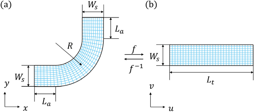
For better understanding of the multimode propagation in conventional waveguide arc-bend, we transform the arc-bend back to a rectangle by CM in reverse. The coordinates of the arc-bend are commonly called physical space, while the coordinates of the rectangle are called virtual space, which are shown in Figs. 1(a) and 1(b). The arc-bend in physical space includes both the waveguide core and cladding areas, which is composed by two additional rectangles with length and width and a 90° arc with radius , while the rectangle in virtual space has length and width .

Fig. 1. CM from the arc-bend in the physical space to a rectangle in the virtual space. (a) The arc-bend is composed by two additional rectangles with length
The CM from physical space to virtual space can be easily obtained by solving Laplace’s equation on the arc-bend in coordinates, with Dirichlet and Neuman boundary conditions [29,30]. We set the inner bend curve as and outer bend curve as , respectively, which correspond to the upper and bottom boundaries of the rectangle in Fig. 1(b). And we set the boundary conditions and for the left and upper straight boundaries of the arc-bend, respectively, which correspond to the left and right boundaries of the rectangle in Fig. 1(b). To ensure and satisfy the Cauchy–Riemann condition of CM, the parameter needs to be optimized. The ratio between and is the optimization objective, which should get close to 1. The Laplace equation-solving and optimization are realized by combining the Laplace and optimization modules in COMSOL Multiphysics software (http://www.comsol.com). Here the optimal is 29.683 μm.
Figure 2(a) shows the refractive index distribution of the arc-bend in the physical space. The width of waveguide is 2 μm, which can support the four lowest-order TE modes. The waveguide core index is 2.84, which is the mode effective index of 220 nm thick silicon slab waveguide with upper cladding, while the index distribution of the rectangle in the virtual space is shown in Fig. 2(b), which is calculated by the equation [22]

Fig. 2. (a) Index distribution of the waveguide arc-bend in physical space. The width of waveguide arc-bend is 2 μm, which can support four TE modes. The waveguide core index is 2.84, which is the 1 ) of CM. This original waveguide is not straight and has a gradient index distribution. These two negative factors cause the big loss and intermode cross talk of the traditional multimode waveguide arc-bend.
According to the analysis of the waveguide arc-bend above, we propose to modify and optimize the original waveguide for multimode propagation in virtual space. This can be simply realized by the waveguide shape-optimizing. Different from previous TO works [14], the optimization and simulation are all implemented in virtual space. Then after a CM, the corresponding MWB in the physical space will be only shape-optimized but without introducing any gradient index distribution. Considering the mirror symmetry along of the original waveguide in Fig. 2(b), the waveguide boundary curves can be expressed in a Fourier cosine series. The expressions of the upper and lower boundary curves and are

Fig. 3. (a) Index distribution of the shape optimized original waveguide in virtual space; (b) index distribution of the MWB in physical space. This MWB has a uniform core index, which makes fabrication easier.
The multimode propagation performance of the shape-optimized original waveguide in virtual space is simulated by the 2D wave-optics module in COMSOL and presented in Fig. 4. Figures 4(a)–4(d) show the profiles of the field component for , , , and modes at 1550 nm wavelength, respectively. All the modes transmit adiabatically in the optimized original waveguide, and no obvious scattering occurs. The simulation results of the shape-optimized MWB in virtual space at 1550 nm wavelength show that the excess losses for the four lowest-order TE modes are less than 0.01 dB and the intermode cross talks are all below .

Fig. 4. Multimode propagation performance of the shape-optimized original waveguide in virtual space. (a)–(d) The profiles of the
We also use rigorous 3D finite-difference time-domain (FDTD) simulations to verify the performance of our shape-optimized MWB in physical space. Figures 5(a)–5(d) show the profiles of the field component for , , , and modes at 1550 nm wavelength, respectively. The insets show the input/output field profiles. Meanwhile, we have simulated the transmission spectra of the four TE modes in the MWB in the wavelength range of 1.1–2.0 μm. To reduce the simulation cost, we divide this broad wavelength range into nine equal subranges to simulate them separately, each with a bandwidth of 100 nm. The material dispersions of silicon and silica have been taken into account in the simulation. We calculate the wavelength-dependence of the coupled power from the th TE mode at the input waveguide to the th TE mode at the output waveguide. Here the excess loss for each mode is given by , while the intermode cross talk is calculated by . To guarantee adequate simulation accuracy, we set the FDTD mesh sizes as , , and . The theoretical transmission spectra of the MWB for , , , and modes are shown in Figs. 6(a)–6(d), respectively. The simulation results at 1550 nm show that excess losses for , , , and modes are only 0.010, 0.010, 0.018, and 0.022 dB, respectively, and intermode cross talks are all below . From these diagrams, we can find that throughout a broad wavelength range of 1.16–1.66 μm, the losses of all modes are below 0.1 dB and the cross talks are all below .

Fig. 5. 3D FDTD simulation results of shape-optimized MWB in physical space. (a)–(d) The profiles of the

Fig. 6. Simulated transmission spectra of shape-optimized multimode bend waveguide. (a)–(d) The spectra for (a)
To evaluate the permitted width fabrication deviation, we introduce a width deviation of the MWB in physical space by moving each point on the boundary shape curve along the outer normal vector at a distance of . The value of varies from to 140 nm with a 20 nm interval. The simulated transmission efficiencies of the shape-optimized MWB at 1550 nm wavelength vary with , as shown in Fig. 7. When the required intermode cross talk is less than , the theoretical permitted width fabrication deviation of our MWB is . This proves that our MWB has large fabrication tolerance.

Fig. 7. Simulated transmission efficiencies of shape-optimized MWB at 1550 nm wavelength vary with the width fabrication deviation
3. FABRICATION AND MEASUREMENT
The proposed shape-optimized MWB was fabricated on an SOI wafer with 220 nm thick top silicon layer and 2 μm thick buried oxide (BOX) layer. The EBL and inductively coupled plasma (ICP) dry etching were applied to fabricate the photonics-integrated circuit (PIC). The micrographs of the fabricated PICs with and without MWB are shown in Figs. 8(a) and 8(b), respectively. A magnified view of MWB is shown in Fig. 8(c). The mode multiplexer and demultiplexer are designed for multiplexing and demultiplexing of the four TE modes (, , , and ) [4].

Fig. 8. Microscopic view of the fabricated PICs and device. (a) The referenced PIC without MWB, including grating couplers, mode multiplexers, and demultiplexers; (b) PIC with MWB; (c) magnified microscopic view of the shape-optimized MWB.
The mode multiplexer and demultiplexer are both formed by the asymmetry directional coupler (ADC) [31,32] between a narrow single-mode waveguide and a wide multimode bus waveguide. The ADC converts the mode of the narrow single-mode waveguide to one higher-order TE mode of the wide multimode bus waveguide, and vice versa. These ADCs are cascaded to realize MDM of the four TE modes. The bus waveguides with different widths are connected through adiabatic tapers, which are long enough to avoid any intermode coupling or radiation loss. Then the bus waveguide is expanded to the final width of 2 μm to access the two cascaded 90° MWBs. After the two MWBs, a mirrored circuit is used to demultiplex different waveguide modes back to mode in different output channels. Grating couplers are used to couple light in and out of the PIC from a single-mode fiber.
A wideband amplified spontaneous emission (ASE) light source covering the C and L bands is used in our measurement. After the output fiber, a commercial 3 dB Y splitter is connected to split the output light into two paths. One is linked to the optical power meter for monitoring and tuning the alignment between the single-mode fibers and the grating couplers. The other is connected to the optical spectrum analyzer (OSA) to measure the transmission spectrum for every mode. To obtain the transmission efficiency of the MWB accurately, the losses of the vertical grating couplers, mode multiplexer, and demultiplexer should be deducted from the measured spectrum of the PIC with MWB. This can be easily done by measuring and subtracting the transmission spectra of the PIC with and without MWB.
The measured transmission spectra for each mode of the shape optimized MWB are shown in Fig. 9. At central wavelength of 1550 nm, the excess losses for , , , and modes are 0.232, 0.327, 0.477, and 0.546 dB, respectively, and intermode cross talks are all below . Since the ASE light source used in the measurement has limited bandwidth of 1520–1620 nm and the 3 dB bandwidth of the grating coupler is only , we could not measure the spectrum of the MWB in the whole wavelength range of 1200–1700 nm. Nevertheless, the transmission spectra for the four TE modes are very flat across the measured wavelength range, which demonstrates our shape-optimized MWB has wide operation bandwidth. The measured transmission efficiencies are slightly lower than the simulated results, which is possibly caused by the waveguide sidewall etching roughness and width random deviation in the fabrication.

Fig. 9. Measured transmission spectra of the shape-optimized MWB for (a)
Table 1 compares the theorical performance of the reported MWBs on a silicon platform. Our MWB demonstrated in this paper has lowest excess losses, widest bandwidth, and sharpest bending among all the four modes channel MWBs. By slightly enlarging the bending radius and the waveguide width, our TO-optimized MWB can also be extended for TM modes or more TE modes. Furthermore, our MWB can be fabricated by one-step lithography and the dry-etching process with large fabrication tolerance.
Table 1. Comparison of Reported MWBs on Silicon Platform (Theoretical Performance)a
|
4. CONCLUSION
In this paper, we demonstrate a compact and broadband MWB supporting four TE modes simply by optimizing the waveguide boundary shape with TO. By designing and optimizing the MWB boundary shapes in virtual space of TO, the loss and intermode cross talk caused by the gradient index distribution are well suppressed. When transformed back to the physical space, the shape-optimized MWB can be formed. The theoretical simulation results show that this shape-optimized MWB exhibits low loss () and low cross talk () across an ultrabroad bandwidth from 1.16 to 1.66 μm, and the permitted waveguide width fabrication deviation is as large as . The proposed MWB was fabricated on a commercial SOI wafer. The measured excess losses for the four lowest-order TE modes are less than 0.6 dB, and the intermode cross talks are all below . This shape-optimized MWB offers great potential to construct densely integrated and wideband MDM systems for on-chip ultrahigh capacity communications. Our proposed TO design method can be expanded to combine with more advanced optimization methods, such as genetic algorithm, particle swarm optimization, and topology optimization. Furthermore, in the future, this method will inspire more integrated TO devices without complicated fabrication.
5 Acknowledgment
Acknowledgment. We thank Dr. Cheng Zeng and the engineer Mr. Pan Li in the Center of Micro-Fabrication and Characterization (CMFC) of WNLO for the support in EBL and ICP dry etching.
Article Outline
Shuyi Li, Lifeng Cai, Dingshan Gao, Jianji Dong, Jin Hou, Chunyong Yang, Shaoping Chen, Xinliang Zhang. Compact and broadband multimode waveguide bend by shape-optimizing with transformation optics[J]. Photonics Research, 2020, 8(12): 12001843.


