Graphene has attracted plenty of attention in the past few years because of its unique electronic structure and exotic properties[1,2]. A significant advantage of graphene is that it can absorb of the incident light over a broad spectral range from ultraviolet (UV) to terahertz[3]. In addition, graphene also shows high carrier mobility (up to )[4,5] and an ultrafast response to optical signals (40 GHz)[6]. However, the responsivity of pure graphene photodetectors is pretty low ()[7]. Other two-dimensional (2D) materials, such as transition metal dichalcogenides (TMDs), have complementary properties to graphene in terms of a direct bandgap in the monolayer and have gained increasing interest as promising photo-active materials for phototransistors. For instance, [8] and [9] photodetectors have shown unprecedented performance with high responsivity and sensitivity. However, the large bandgap of TMDs corresponds to the visible spectral range[10,11], making them not suitable for detecting infrared light, especially the optical signal at the telecommunication wavelength (e.g., 1550 nm). Therefore, it is very necessary to search for new 2D materials that are suitable for broadband photodetection.
Black phosphorus (BP) is a layered semiconducting material in which each phosphorus atom is bonded to three neighboring phosphorus atoms within the plane[12]. BP has a direct bandgap from 0.3 eV (bulk) to 1.8 eV (monolayer), which is independent of the layer numbers[1315" target="_self" style="display: inline;">–15], making it an appealing candidate for broadband detection from visible to infrared wavelengths. In addition to its small bandgap, BP flakes also show impressively high carrier mobility from (in flakes)[14] to 10000 (in bulk) [16], superior to most TMDs, affording intriguing potential for ultrafast optoelectronic applications. Additionally, unlike graphene, BP flakes also have an anisotropic micro-structure, which allows the realization of novel nano-optical devices that are sensitive to polarized light. The first BP photodetector was reported by Buscema et al., but the device showed a relatively low responsivity of [15]. After that, many efforts have been made to increase the performance of BP photodetectors. In particular, Wu et al. demonstrated a BP photodetector operating at UV wavelengths with a very high responsivity of [17]. Recently, a high-performance broadband BP photodetector was fabricated by Huang et al., operating in the wavelength range from 400 to 900 nm. The device showed a high responsivity of at 633 nm[18]. However, it is noteworthy that a highly efficient BP-based infrared photodetector operating at 1550 nm has not been demonstrated.
Here, we present an efficient broadband photodetector using thin BP flakes as a light-absorbing material. The mechanically exfoliated BP crystals are a few nanometers in thickness and about 10 μm in lateral size. Comparing to pure graphene-based photodetectors, our BP-based photodetector devices show significantly improved performance in terms of responsivity in a wide wavelength range from visible to infrared. An ultrahigh responsivity () at the telecommunication wavelength (1550 nm) with a rise time of 4.8 ms and a fall time of 6.8 ms was achieved, making it very attractive for infrared imaging and optical communication.
We exfoliated the BP flakes from a synthetic bulk BP crystal (Smart Elements GmbH) with bule Nitto tape (Nitto Denko Co., SPZ 224P). By using the all-dry transfer technique[19], thin BP flakes were then transferred onto a -doped Si substrate with a 300 nm thick insulating layer. We used electron-beam evaporation with a shadow mask that has a channel of 8 μm to form the device structure and metals.
The surface morphology of the BP nanoflakes was examined by a scanning electron microscope (SEM, Carl Zeiss, Supra 55). The thickness of the BP nanoflakes was measured using atomic force microscopy (AFM, Bruker, Dimension Icon). The Raman spectrum was collected on a micro-Raman system (Horiba Jobin Yvon, LabRAM HR 800) with a 514 nm excitation laser.
The photodetection experiments at a visible wavelength (635 nm laser) and a near-infrared wavelength (980 nm laser) were performed on a probe station (Cascade M150) equipped with a semiconductor property analyzer (Keithley 4200). The photodetection measurements at 1550 nm were performed using a NeaSpec optical microscope platform, which is able to couple and focus the infrared light beam onto the desired location of the BP photodetector. Then, the photocurrent was collected by a Keithley (2614B) double-channel source meter. During the whole device fabrication process, the sample was kept in the glove box. The photodetection measurements were conducted in vacuum conditions.
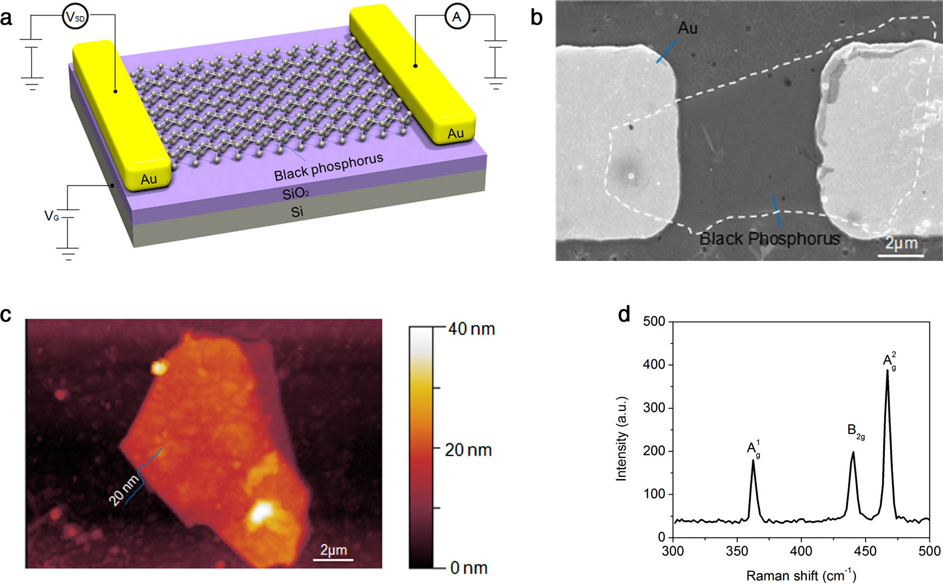
Figure 1(a) shows the schematic configuration of our BP photodetector device. The SEM image of the BP photodetector is shown in Fig. 1(b). We can see that the morphology of the BP flakes is uniform, and the length of the BP flakes is about 12 μm. The width of the BP flakes is averaged from the leftmost to the rightmost part, and the average value is about 5 μm. Figure 1(c) illustrates a representative AFM image of an exfoliated BP flake, showing a thickness of . We also measured other BP flakes with different shapes; most of them have a thickness of 20–30 nm. To further confirm the microstructure of the BP flakes, the Raman spectrum was taken, as shown in Fig. 1(d). Under the excitation of a 514 nm laser, the Raman peaks of thin-film BP can be identified at the low frequency region at 365, 440, and , corresponding to the , , and , vibration modes of the BP lattice.
Fig. 1. (a) Schematic illustration of the BP photodetector. (b) SEM image of the BP photodetector with Au electrodes. (c) AFM image of BP nanoflakes showing a thickness of . (d) Representative Raman spectrum of BP.
下载图片 查看所有图片
We then investigated the photoresponse of the as-fabricated BP photodetector. Figure 2(a) displays the photocurrent of the BP photodetector as a function of the source-drain voltage () without gate voltage under different laser powers (excitation wavelength: 635 nm). It is found that the photocurrent increases as varies from 0 to 0.5 or because of the increased carrier drift velocity and the reduced carrier transit time[8]. The nonlinear dependence of the photocurrent on illustrates the existence of a Schottky barrier between BP and gold. We found that the photocurrent increases as the laser power increases from 100 to 500 nW. This is because stronger incident light enables the generation of more electron-hole pairs, which leads to a rise in the photocurrent.
Fig. 2. (Color online) (a) Power-dependent photocurrent as a function of source-drain voltage () at 635 nm. (b) Energy diagram illustrating the photocurrent generation with and without bias. (c) Gate-tunable source-drain current () with and without light illumination. Laser wavelength: 635 nm, . (d) Time-dependent photocurrent at 635 nm with a light power of 400 nW. . (e) Rise time (10% to 90%) and fall time (90% to 10%) of BP photodetector device at 635 nm. (f) Photocurrent and responsivity as functions of the incident light power at 635 nm.
下载图片 查看所有图片
The energy diagram in Fig. 2(b) can explain the photocurrent generation process in the BP photodetector. The top panel of Fig. 2(b) donates the metal-semiconductor contact without light illumination and the bias voltage between the Au electrodes and BP. It is known that the work function of Au is [20], and the work function of BP (20 nm) is [21]. Therefore, when they have contact with each other, there will be a band bending at the interface. As a result, two metal-BP Schottky junctions (Au-BP and BP-Au junctions) are formed, and the Schottky barrier hinders the effective carrier injection. However, the case can be different with external bias and under light illumination, as shown in the bottom panel of Fig. 2(b). When an external voltage was applied to the device, a forward bias will form in one junction, while a reverse bias will form in the other. The forward bias reduces the Schottky barrier at the junction and allows more electrons to reach the electrode easily. When the device is exposed to light, electrons from the valence band (VB) of BP can be easily excited to the conduction band (CB) by incident photons. Then, the holes and electrons are separated by the built-in electrical field. Specifically, electrons move to the side of the electrodes where a forward bias occurs, which, in turn, further reduces the barrier and contributes to a larger photocurrent.
Figure 2(c) shows the source-drain current () as a function of the gate voltage with and without incident light at a fixed of 0.1 V. We can observe a higher current () at the negative gate voltage () in the transfer curve, indicating the -type transport characteristic in BP. Under the illumination of a 400 nW laser, the current () increases dramatically, and a photocurrent of was obtained while . A time-dependent photoresponse has been obtained using the 635 nm laser with a power of 400 nW, as shown in Fig. 2(d). The photocurrent can be effectively switched on and off as the light source is turned on and off, and we can get a stable photocurrent in the “on” state at a of 0.1 V. Then, we can extract the rise time and fall time of our photodetector, as shown in Fig. 2(e). The result reveals a rise time of 7.8 ms (from 10% to 90%) and a fall time of 20 ms (from 90% to 10%), which can meet the requirements of many optoelectronic applications. We also plotted the power-dependent photocurrent and calculated the responsivity at 635 nm, as shown in Fig. 2(f). As the incident laser power increases from 100 to 400 nW, the photocurrent increases almost linearly, while the corresponding responsivity decreases nonlinearly. Under the illumination of 100 nW laser power, we can get a high responsivity of , which is times larger than that of a pure graphene-based photodetector[7].
To investigate the capacity of infrared light detection, we measured the photoresponse of our device at 980 and 1550 nm, as shown in Fig. 3. The power-dependent as a function of at the wavelength of 980 nm is shown in Fig. 3(a). also increases with the increase of the laser power, similar to the scenario under visible light excitation. Figure 3(b) is the time-dependent photocurrent with different laser powers from 0.5 to 2 μW at 980 nm (). Under the illumination of 2 μW light, we can get a stable photocurrent of . The photocurrent decreases as the incident light power decreases. It can be seen that the photocurrent with different incident light powers can be effectively turned on and off as the light is switched on and off. We also calculated the photocurrent and responsivity at 980 nm, and the results are shown in Fig. 3(c). It is also revealed that the responsivity decreases as the incident light power increases. Under the illumination of 500 nW light, we can get a high responsivity of .
Fig. 3. (Color online) (a) Power-dependent source-drain current () as a function of the source-drain bias () at 980 nm. Inset is a zoom in of the curve. (b) Time-dependent photocurrent under different incident light powers at 980 nm. . (c) Photocurrent and responsivity as functions of the incident light power at 980 nm. (d) Time-dependent photocurrent with varying incident light powers at 1550 nm. . (e) Rise time (10% to 90%) and fall time (90% to 10%) of our device at 1550 nm. (f) Photocurrent and responsivity as functions of the incident light power at 1550 nm.
下载图片 查看所有图片
The photoresponse of our device under the illumination of 1550 nm light is shown in Figs. 3(d)–3(f). The time-dependent photocurrent curve was performed using different laser powers at a fixed of 1 V, as shown in Fig. 3(d). It is clearly seen that the photocurrent of the BP photodetector is very stable and increases as the laser power increases. The photocurrent increases from 2.5 to 17.5 μA when the laser power increases from 11 to 211 nW. Figure 3(e) shows the rise time and fall time of the BP photodetector at 1550 nm, showing a rise time of and a fall time of . The photocurrent and responsivity as a function of the illumination light power are also studied, and the results are shown in Fig. 3(f). The photocurrent increases nonlinearly, while the responsivity decreases exponentially while promoting the incident power. That is because the increase of photoexcited carriers caused by the higher incident power will produce an electrical field opposite to the built-in field at the interface of the Au electrodes and BP, which will hinder the separation and transport of photogenerated electron-hole pairs. We can get a responsivity as high as at a light power of 11 nW, which is about times higher than that of a pure graphene photodetector [7], times higher than that of a pure BP photodetector ()[22], and about times higher than an InP photodetector[23] at this particular wavelength, as shown in Table 1.
Table 1. Comparison of Our BP Photodetector with Previously Reported BP Photodetectors
| Material | (V) | (V) | Thickness (nm) | Spectral range (nm) | Response time (ms) | Responsivity | References |
|---|
| BP | 1 | 0 | 20 | 1550 | 4.8 | | This work | | BP | 0.2 | 0 | 8 | 640 | 1 | | [15] | | BP | | | 8 | 900 | – | | [18] | | BP | | 0 | 120 | 1550 | – | | [22] | | BP | | | 11.5 | 1550 | | | [24] | | 3 | 60 | 22/12 | 1550 | | | [25] | | InP | 7 | 0 | | 1550 | – | | [23] |
|
查看所有表
In conclusion, we have successfully demonstrated a highly efficient BP-Au Schottky-type photodetector which can operate in a broadband wavelength from visible (635 nm) to infrared wavelengths (1550 nm). Under the illumination of the telecommunication light at 1550 nm, BP photodetector shows an ultrahigh responsivity of , which outperforms previous reports on pure BP photodetectors. A fast rise time of 4.8 ms and a fall time of 6.8 ms were also observed in the BP photodetector. The unprecedented performance of the BP photodetector indicates great potential for infrared imaging and optical communication applications.
Yan Liu, Tian Sun, Weiliang Ma, Wenzhi Yu, Shivananju B. Nanjunda, Shaojuan Li, Qiaoliang Bao. Highly responsive broadband black phosphorus photodetectors[J]. Chinese Optics Letters, 2018, 16(2): 020002.
 Download: 960次


