Photonics Research, 2019, 7 (8): 08000868, Published Online: Jul. 17, 2019
Experimental demonstration of an electrically tunable broadband coherent perfect absorber based on a graphene–electrolyte–graphene sandwich structure  Download: 511次
Figures & Tables
Fig. 1. (a) Schematic view of a GSS illustrated by two counter-propagating and coherently modulated input beams (I + I − O + O −
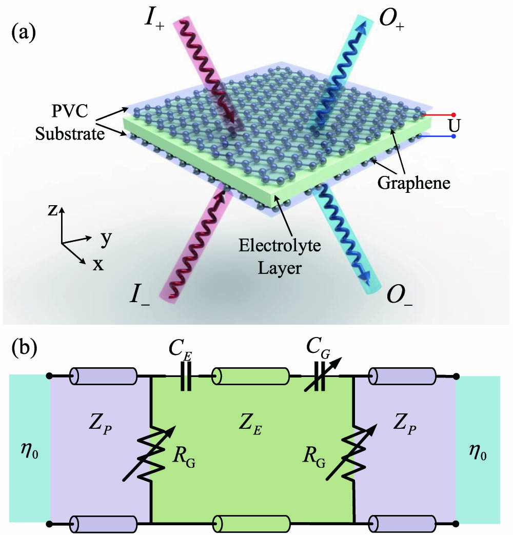
Fig. 2. Coherent absorption of GSS for plane wave versus frequency under different Fermi levels. The solid line represents the 3D full wave simulation results and dotted line means the equivalent circuit calculated results.

Fig. 3. Two-dimensional false-color plot of the calculated coherent absorption as a function of Fermi level and phase modulation. (a) Equivalent circuit calculated results and (b) simulated results.

Fig. 4. (a) and (b) Calculated coherent absorption under TE/TM incident illumination, where the dashed lines denote the condition of E F = 0.22 eV

Fig. 5. Coherent absorption of N -layers stacked GSS versus Fermi energy. Insert graph is the schematic of stacked GSS illuminated by two counter-propagating input beams. Solid curves represent the equivalent circuit calculated results and triangles refer to the full-wave simulation results.

Fig. 6. (a) Optical image of graphene on a PVC substrate. (b) Raman spectrum of monolayer graphene. (c) Fabricated GSS device. (d) Configuration of the waveguide measurement setup. (e) Relation between the Fermi level of graphene and bias voltage.

Fig. 7. (a) Measured (circles) and calculated (solid lines) coherent absorptivities of GSS in the waveguide system under different bias voltages. (b) A 2D false-color plot of the coherent absorptivity as a function of frequency and phase modulation (U = 3 V f = 4.27 GHz

Jin Zhang, Xingzhan Wei, Malin Premaratne, Weiren Zhu. Experimental demonstration of an electrically tunable broadband coherent perfect absorber based on a graphene–electrolyte–graphene sandwich structure[J]. Photonics Research, 2019, 7(8): 08000868.


 PDF全文
PDF全文

