Photonics Research, 2014, 2 (3): 03000A41, Published Online: Nov. 5, 2014
Efficient adiabatic silicon-on-insulator waveguide taper  Download: 1137次
Abstract
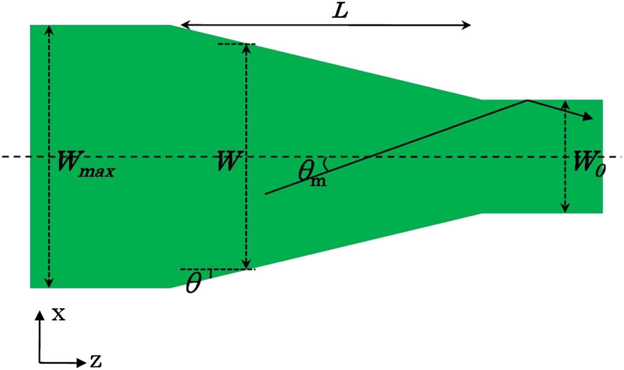
A silicon-on-insulator-based adiabatic waveguide taper with a high coupling efficiency and small footprint is presented. The taper was designed to reduce the incidence of mode conversion to higher-order and radiation modes inside the waveguide. In connecting a 0.5-μm-wide output waveguide and a 12-μm-wide input waveguide of a grating coupler, a compact 120-μm-long taper was demonstrated, achieving a transmission of 98.3%. Previously, this transmission level could only be achieved using a conventional linear taper with a length of more than 300 μm.
Yunfei Fu, Tong Ye, Weijie Tang, Tao Chu. Efficient adiabatic silicon-on-insulator waveguide taper[J]. Photonics Research, 2014, 2(3): 03000A41.


