1. INTRODUCTION
Silicon photonics is deemed to be a promising solution for future high-speed on/off-chip optical interconnections [1], owing to its fabrication compatibility with complementary metal-oxide semiconductor processes and the small footprints of silicon photonic devices. In compact silicon photonic devices, the width of the silicon waveguides is usually as narrow as 0.5 μm because of the high refractive index contrast between the silicon core () and the cladding (). However, the waveguides in different devices are likely to be designed with different cross-sections in order to achieve better performances. Even in a single device, waveguides are also likely to be designed with different cross-sections to realize different functions, including arrayed-waveguide gratings [2], multimode interference couplers [3], grating couplers [4,5], and crossings [6]. In addition, silicon waveguide tapers are also directly used as spot-size converters to connect the silicon photonic waveguides with external fibers or optical dyes [7]. Thus, designing a better waveguide taper for obtaining an efficient coupling between two different optical waveguides is a very important issue in silicon photonics research. This aspect has been extensively studied and discussed in the literature [810" target="_self" style="display: inline;">–10].
Normally, the function of the taper is to change the size and the shape of the optical mode to achieve a high coupling efficiency between two waveguides with different cross-sections. To do this, the taper must operate adiabatically; that is, the local first-order mode of the waveguide should propagate through the taper while undergoing relatively little mode conversion to higher-order modes or radiation modes. This adiabatic operation can be realized in the taper design by increasing/decreasing the size of the taper cross-section very slowly.
Many designs of adiabatic tapers have been proposed for silicon-on-insulator (SOI)-based photonic devices, including linear [2–5" target="_self" style="display: inline;">–5], exponential [6], parabolic [11], and Gaussian [12] expansion types. In general, a linear waveguide taper is used to connect two optical waveguides with different cross-sections. In this linear adiabatic taper, mode conversion occurs more easily in the wider portion [10]. If a low-loss transmission is needed, the linear adiabatic taper must be extended to be long enough to achieve an adiabatic propagation. However, a longer taper leads to more propagation losses. This problem will become more critical when the two waveguides connected by the linear taper have a great difference in their cross-sections. For example, a grating coupler, which is a prospective wafer-scale test device, typically has a 12-μm-wide waveguide. The adiabatic propagation between a 12-μm-wide waveguide and a single-mode 0.5-μm-wide waveguide requires that the linear taper must be longer than 400 μm. A large number of grating couplers will be used for online wafer testing in the production of silicon photonic devices; as a result, a large wafer area will be occupied by the linear tapers. Therefore, to lower the fabrication costs and achieve high-density integration, the footprint of the taper should be reduced; for this purpose, efficient and compact tapers are needed. A number of research studies on compact tapers have been presented in the literature. The approaches discussed in these works can be classified into three categories: nonadiabatic planar waveguide tapers [1315" target="_self" style="display: inline;">–15], lens-assisted focusing tapers [16], and discontinuous tapers [17].
In 2004, Luyssaert et al. proposed a nonadiabatic waveguide taper with a length of 15.4 μm. An experiment using this taper resulted in a transmission of 70% [15]. However, the principle of the nonadiabatic taper is very complex and we failed to find further reports on this structure. Van Acoleyen and Baets proposed a lens-assisted focusing taper containing an in-plane lens [16]. For a 20-μm-long lens-assisted focusing taper, losses of about 1 dB (TE-like mode) and 5 dB (TM-like mode) were experimentally measured. In a discontinuous taper, 90% transmission is obtained by a 3-D vectorial mode solver of the fundamental TM-like mode [17]. Nevertheless, in these designs, the coupling efficiencies of the tapers are still not high enough. Therefore, more efficient and compact tapers are still needed.
In this work, we propose an efficient adiabatic taper with a small footprint based on an SOI substrate. The details of the design and optimization are studied. A adiabatic taper used to connect a grating coupler and a single-mode waveguide is demonstrated with a taper length of 120 μm and a transmission of 98.3%.
2. THEORY
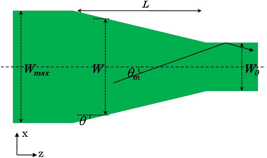
In 1977, Milton and Burns proposed a simple design rule to ensure adiabatic operation in a symmetric Ti-diffused taper [9,10]. In a taper designed using this rule, the lowest-order optical mode is well confined by side walls. The taper should be designed to conform with the equation where is the local half angle of the taper at the point , is the wavelength in vacuum, is the mode effective index of the mode, and is the local full width of the taper at point , as shown in Fig. 1.
Fig. 1. Top view of the structure of a linear waveguide taper. is the width of the single-mode waveguide, is the maximum taper width, is the length of the taper, is the local half angle of the taper at point , and is the projection of the ray angle of the first-order mode of the taper.
下载图片 查看所有图片
The rule requires that the spreading of the waveguide sidewalls be slower than the diffraction spreading of the lowest-order (first-order) mode. Accordingly, the first-order mode will be confined in the taper without mode conversion to higher-order modes or radiation modes. Using a ray model to describe the mode propagation, is consequently defined as the projection of the ray angle of the first-order mode of the taper, and is defined as the taper angle. If in the ray model, the ray would not reach the boundary of the waveguide taper and the phase front of the wave would become distorted, resulting in a mode conversion from the first-order local normal mode to higher-order modes [10].
3. DESIGN
In this work, we use the rule derived by Milton and Burns to design an efficient adiabatic SOI taper. The taper is based on an SOI wafer with a 220-nm-thick top silicon layer and a 2-μm-thick buried oxide layer.
Here, to investigate the adiabatic condition of the SOI taper, we insert a constant into Eq. (1):
Using Eq. (2), we designed a taper connecting a 2.0-μm-wide input waveguide and a 0.5-μm-wide output waveguide. Lumerical mode solutions is used in simulation, with the grid sizes set to less than 1 nm. The calculated transmission dependence on the constant of the silicon waveguide taper is shown in Fig. 2. For , a transmission of more than 98% was achieved. However, as increased, the transmission of the taper decreased, and this reduction was rapid when reached and crossed 1.5. Taking into account the calculated results for the mode field intensity, we suggest that the reason for this result is the transfer of a large amount of power from the first-order mode to higher-order modes and radiation modes above . From the simulated results, we can see that an SOI taper designed with can achieve a high transmission of above 98%, which does not agree with the rule derived by Milton and Burns. Considering that high-accuracy simulations of this type were not available in the 1970s, we believe that the adiabatic condition for an SOI taper can be expanded to .
Fig. 2. Transmission dependence on the constant of the silicon waveguide taper designed using Eq. (2), at a wavelength of 1550 nm.
下载图片 查看所有图片
In design, we can choose the constant according to the desire of photonic device. A smaller constant is chosen if a higher transmission (smaller amount of mode conversion) is desired, resulting in a longer taper. In contrast, a larger resulted in a lower transmission but a shorter taper.
In addition, the transmission of the taper designed using Eq. (2) was investigated for different lengths. For comparison, linear, parabolic, exponential, and Gaussian types of taper were added, as shown in Fig. 3. All tapers expanded to the same maximum width over the same length, which varied from 1 to 6 μm. The width of the input and output waveguides were 2.0 and 0.5 μm, respectively.
Fig. 3. Transmission of a taper designed according to Eq. (2) as a function of the length of the taper. For comparison, linear, parabolic, exponential, and Gaussian taper types are included.
下载图片 查看所有图片
It was found that a 1.5-μm-long adiabatic taper achieves a transmission of approximately 96%. Furthermore, the taper was almost lossless when it was longer than 2 μm. However, a 1.5-μm-long linear taper could only obtain an 85% transmission; moreover, the transmission values of the parabolic, exponential, and Gaussian tapers of the same length were worse than the linear taper. A 3-μm-long linear taper produces a similar transmission, 96%, but with a length double that of the adiabatic taper we designed. It is clear that our designed adiabatic taper exhibits better performance in the simulated range than the other types of tapers of the same length.
In Fig. 4, we show the numerical calculation of the field intensity of the various tapers at a wavelength of 1550 nm. The input light source was set with a first-order mode and TE polarization. In Fig. 4(a), we do not see indications that the first-order mode is converted to higher-order modes or radiation modes in the designed adiabatic taper. However, the exponential, parabolic, Gaussian, and linear taper obviously do not exhibit adiabatic propagation, as shown in Figs. 4(b)–4(e). Finally, in Fig. 4(f), a much lower amount of mode conversion from the first-order mode to higher-order or radiation modes can be seen in the case of the 15-μm-long linear taper.
Fig. 4. Simulated field intensity for the various tapers at a wavelength of 1550 nm. (a) 5-μm-long adiabatic taper designed using Eq. (2), (b) 5-μm-long exponential taper, (c) 5-μm-long parabolic taper, (d) 5-μm-long Gaussian taper, (e) 5-μm-long linear taper, and (f) 15-μm-long linear taper.
下载图片 查看所有图片
As such, a 15-μm-long linear taper might be acceptable. However, when the width of input waveguide is significantly larger than the width of the output waveguide, the linear taper will have to be designed very long to achieve adiabatic propagation. Currently, a linear taper connected a 12-μm-wide grating coupler and a 0.5-μm-wide single-mode silicon waveguide must be longer than 400 μm to achieve low-loss propagation. The transmissions of our designed taper and the other taper types are shown in Fig. 5. The simulated results show that a 120-μm-long adiabatic taper can achieve a transmission of 98.3%, a value which can also be reached by a linear taper longer than 300 μm. For a parabolic taper, the transmission tends to fluctuate as it rises with increasing taper length. At some lengths, the parabolic taper exhibits a high performance, closely approximating that of our designed taper, which is a result of the adiabatic and parabolic tapers having a similar profile shape.
Fig. 5. Transmission of the tapers as a function of taper length at a wavelength of 1550 nm. The widths of the input and output waveguides are 12 and 0.5 μm, respectively.
下载图片 查看所有图片
The designed taper is also studied for different thicknesses, which are widely used in silicon photonics. Figure 6 shows the simulated transmission of the designed taper as a function of taper length for different taper thicknesses for the fundamental TE mode at a wavelength of 1550 nm. The widths of the input and output waveguides were 12 and 0.5 μm, respectively. The designed taper can achieve a transmission of more than 97% for a taper length of 100 μm. Note that for a certain taper length less than 100 μm, a 340-nm-thick taper has a transmission lower than that of a 220-nm-thick taper. This is because the mode effective index of the fundamental TE mode of the 340-nm-thick taper is larger than that of the 220-nm-thick taper, which consequently results in a larger . In summary, the designed taper can also achieve a high performance with SOI wafers with 260, 300, and 340 nm thicknesses at a short length.
Fig. 6. Transmission of the designed taper for different taper thicknesses as a function of taper length, for the fundamental TE mode at a wavelength of 1550 nm.
下载图片 查看所有图片
4. CONCLUSION
An efficient SOI-based adiabatic taper is proposed in this work. The first-order mode is well confined in the adiabatic taper without conversions to higher-order and radiation modes. For , the SOI adiabatic taper can achieve a high transmission of above 98%. For connecting a 12-μm-wide grating coupler and a 0.5-μm-wide single-mode silicon waveguide, a 120-μm-long adiabatic taper achieves a high transmission of 98.3%, which can only be reached by a conventional linear taper with a length longer than 300 μm. The designed taper exhibits better performance than the linear, parabolic, exponential, and Gaussian taper types. The adiabatic taper also exhibits good performance for 220–340-nm-thick SOI wafers. Compared to widely used linear tapers, this adiabatic taper can greatly reduce the SOI wafer area used to realize high-density photonic integration.
Yunfei Fu, Tong Ye, Weijie Tang, Tao Chu. Efficient adiabatic silicon-on-insulator waveguide taper[J]. Photonics Research, 2014, 2(3): 03000A41.
 Download: 1136次


