1. INTRODUCTION
III-nitride ultraviolet (UV) laser diodes (LDs) have been attracting intense research interest due to their great application prospects in medical sterilization, biological analysis, high-security military communication, and so on [1–7" target="_self" style="display: inline;">–7]. Compared with conventional LDs with Fabry–Perot cavities, microdisk LDs with low-loss whispering gallery modes (WGMs) have many advantages in small mode volume, high quality factor, and low threshold [810" target="_self" style="display: inline;">–10]. Therefore, the III-nitride UV microdisk LD has emerged as a hot research field in the past few years [1113" target="_self" style="display: inline;">–13]. In particular, III-nitride UV microdisk LDs grown on large-size, cost-effective Si substrates open up a new platform for UV photonics integration [14–17" target="_self" style="display: inline;">–17].
Conventional III-nitride microdisk LDs employ a “mushroom-like” architecture featured with an undercut structure, which, however, has several crucial drawbacks, such as impractical electrical current injection with an extremely large series resistance, very short lifetime with limited heat dissipation, and device processing instability with poor uniformity [18–21" target="_self" style="display: inline;">–21].
In our previous work, we proposed and fabricated a “sandwich-like” architecture with both upper and lower AlGaN cladding layers to confine the optical field, and demonstrated room-temperature electrically pumped InGaN-based violet microdisk lasers grown on Si [22]. The reported lasing wavelength was 412.4 nm, and the radius of the as-fabricated microdisk laser was 20 μm. In this study, to extend the lasing wavelength to UV range, we significantly reduced the indium content in the InGaN-based quantum wells (QWs) and increased the aluminum content in the AlGaN cladding layers to ensure optical confinement. To shrink the size of the UV microdisk LD, we adopted an air-bridge electrode structure for realizing electrical pumping, because it is challenging to inject current for microdisk LDs with a radius of less than 20 μm through a regular probe. The result is the first demonstration, to the best of our knowledge, of room-temperature electrically injected GaN-based near-UV (NUV) microdisk LDs with a radius of 12 μm grown on Si.
2. MATERIAL GROWTH AND CHARACTERIZATION
III-nitride semiconductor materials are significantly different from Si substrates in both lattice constant and coefficient of thermal expansion (CTE), which usually lead to a high density of dislocations and a large tensile stress, respectively [16,23–26" target="_self" style="display: inline;">–26]. The tensile stress generated during the cooling process to room temperature often results in a huge wafer bow and even micro-crack networks. Threading dislocations often act as non-radiative recombination centers, which are detrimental to internal quantum efficiency (IQE) and LD device performance. For NUV LDs particularly, only a little indium is incorporated in the NUV QWs, inducing limited localization states in both state density and potential fluctuation, which affects the IQE of the active region substantially [15]. Therefore, it is of great significance to reduce the threading dislocation density (TDD) and mitigate the tensile stress for building NUV microdisk LDs on Si.
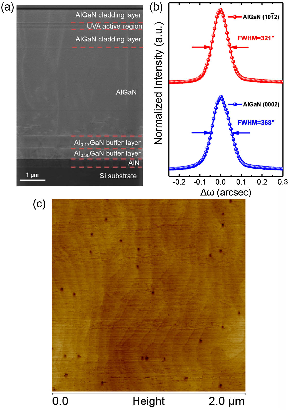
An Al-composed graded AlN/AlGaN multilayer buffer was adopted to circumvent the lattice mismatch and CTE misfit problems for the growth of a thick n-type AlGaN film on Si substrates. The 6.5-μm-thick crack-free NUV LD structure [Fig. 1(a)], including optical cladding layers, waveguide layers, active region, electron block layer, and contact layer, was then overgrown on the n-AlGaN template. The detailed information of the individual layers can be found in our previous work [15]. The crystalline quality of the as-grown n-AlGaN film on Si was evaluated by double crystal X-ray rocking curve measurements [Fig. 1(b)]. The full widths at half-maximum (FWHMs) of (0002) and (102) planes of the n-AlGaN template were 368 and 321 arcsec, respectively, which give an estimate of the n-AlGaN TDD of . This is consistent with the observation of atomic force microscopy (AFM), as shown in Fig. 1(c).
Fig. 1. (a) Cross-sectional transmission electron microscopy (TEM) image, (b) double crystal X-ray rocking curves for the AlGaN (0002) and (102) planes of the NUV LD structure grown on Si, and (c) AFM surface image of the AlGaN grown on Si.
下载图片 查看所有图片
3. FABRICATION OF MICRORING AND MICRODISK LASER DIODES
The as-grown NUV laser wafer was fabricated into two types of devices, microring LDs and microdisk LDs with air-bridge electrodes (Fig. 2). Figure 2(a) illustrates the structure of a microring LD that contains an inner circle with a insulation layer underneath to confine the current injection only through the annular region. Figure 2(b) shows a scanning electron microscopy (SEM) image of one as-fabricated microring LD with an outer () and inner () radius of 20 and 10 μm, respectively. For the electrical testing of microdisk LDs with a radius of less than 20 μm, the size of the device pads is too small to put a regular probe pin on the p-type contact metal for direct current injection. Therefore, the air-bridge electrode structure connecting the p-type contact of the small microdisk LD with a large square metal pad was designed for the convenience of device testing. The schematic of the microdisk LDs with air-bridge electrodes is shown in Fig. 2(c), and it should be mentioned that the light output around the microdisk is just a sketch, which does not necessarily represent the real light output paths. Figure 2(d) presents an array of as-fabricated microdisk LDs with air-bridge electrodes.
Fig. 2. (a), (c) Schematics and (b), (d) SEM images of the (a), (b) microring LD and (c), (d) microdisk LDs with air-bridge electrodes.
下载图片 查看所有图片
The fabrication process flow of the air-bridge electrode structure is illustrated in Fig. 3. First, photolithography and inductive coupled plasma (ICP) etching were used to pattern and form the microdisk LDs covered with p-contact metal and the square-shaped mesa covered with a insulation layer to serve as the mechanical support of the extended p-contact metal pad [Fig. 3(a)]. Second, photoresist and photolithography were implemented to form a mechanical support for the subsequent n-contact metal deposition on the photoresist, as well as the exposed n-AlGaN surface, the p-contact metal, and the square mesa covered with [Figs. 3(b) and 3(c)]. The n-type ohmic contact metal stack consisted of Ti, Pt, and Au with thicknesses of 50, 100, and 500 nm, respectively. Third, another level of photolithography and ion beam etching was then employed to pattern and define the air-bridge metal structure, as shown in Fig. 3(d). Finally, the remaining photoresist was lifted off by acetone, ethanol, and deionized water to realize the air-bridge electrode structure [Fig. 3(e)].
Fig. 3. Schematic process flow of the microdisk LD structure with an air-bridge electrode.
下载图片 查看所有图片
It should be mentioned that in order to remove the ICP etching-induced damages and chemically polish the rough sidewalls of the microring and microdisk LDs, tetramethyl ammonium hydroxide (TMAH) solution etching was implemented at the end of the process flow for all the as-fabricated devices. It was confirmed that the TMAH treatment significantly reduced non-radiative recombination and optical loss, as well as threshold current [22,27].
4. CHARACTERIZATION OF DEVICES
Due to the air-bridge electrode structure, the electrical testing of the small microdisk LDs became straightforward. The electroluminescence (EL) of one as-fabricated GaN-based NUV microdisk LD with a radius of 12 μm grown on Si was measured under a pulsed electrical injection at room temperature, as shown in Fig. 4. The pulse width and repetition rate were 400 ns and 10 kHz, respectively. Figure 4(a) shows the EL spectra of the microdisk LD under various pulsed currents. The device gave a broad spontaneous emission around 386 nm under a low injection. A stimulated emission at 386.3 nm was observed at 248 mA. Figure 4(b) shows the variation of the FWHM of the EL spectra and the integrated EL intensity, as the injection current was increased gradually from 100 to 292 mA. When the injection reached the threshold current (Ith) of 248 mA, the FWHM of the emission spectrum quickly narrowed down to 0.9 nm, and the integrated EL intensity increased super-linearly. These observations demonstrate an electrically injected lasing operation from the NUV microdisk LDs grown on Si with a lasing wavelength of 386.3 nm at room temperature.
Fig. 4. (a) EL spectra of the microdisk LD with a radius of 12 μm measured under various pulsed electrical currents. (b) FWHM of the EL spectra and integrated intensity of the EL spectra as a function of the injection current. The pulse width and repetition rate were 400 ns and 10 kHz, respectively.
下载图片 查看所有图片
For the microring LDs with an outer circle radius, , of 20 μm, the device characterization was carried out by directly probing the p-contact metal pad. As the radius of the inner current blocking circle increases, the threshold current (Ith) of the microring LDs decreases significantly (Fig. 5). In the presence of the inner current blocking circle with the insulation layer underneath, electrical current can inject only from the annular region of the microring LDs. When the inner circle gets larger, the current injection gets closer to the periphery of the microring LDs, giving increased contribution to the gain for stimulated emission, because the WGMs propagate only along the periphery. In contrast, the current injection into the region away from the periphery with a smaller inner current blocking circle can generate spontaneous emission or heat only through radiative or non-radiative recombination, respectively, but makes little contribution to the WGMs. It should be noted that there was no current blocking inner circle in the as-fabricated small microdisk LDs with air-bridge electrodes, and hence current was injected through the entire microdisk. Therefore, it is expected that the threshold of the microdisk LDs can be further reduced by adopting microring structure with the current blocking design, which would require advanced lithography in future work.
Fig. 5. Threshold current, Ith, as a function of the inner circle radius for the microring LDs with an outer circle radius, , of 20 μm.
下载图片 查看所有图片
5. CONCLUSION
In summary, room-temperature electrically pumped GaN-based NUV microdisk LDs with a radius of 12 μm have been achieved through the epitaxial growth of a 6.5-μm-thick NUV laser structure on Si substrates with an Al-composed graded AlN/AlGaN multilayer buffer, and the fabrication of sandwich-like microdisk structure with air-bridge electrodes. Further enhancement in device performance can be obtained by improving the material quality, strengthening the optical confinement, and applying microring structure with current blocking for the central region of the microdisk LDs.
6 Acknowledgment
Acknowledgment. We are thankful for the technical support from Nano Fabrication Facility, Platform for Characterization & Test, and Nano-X of SINANO, CAS.
Jin Wang, Meixin Feng, Rui Zhou, Qian Sun, Jianxun Liu, Yingnan Huang, Yu Zhou, Hongwei Gao, Xinhe Zheng, Masao Ikeda, Hui Yang. GaN-based ultraviolet microdisk laser diode grown on Si[J]. Photonics Research, 2019, 7(6): 06000B32.
 Download: 542次


