Photonics Research, 2019, 7 (9): 09000955, Published Online: Aug. 2, 2019
Active control of EIT-like response in a symmetry-broken metasurface with orthogonal electric dipolar resonators  Download: 545次
Figures & Tables
Fig. 1. (a) Schematic and (b) photograph of the symmetry-broken metasurface. The metallic pattern is copper with a conductivity of 5.8 × 10 7 S / m 72.14 mm × 34.04 mm × 1.0 mm 4 × 10 − 4 L 1 = 32 mm L 2 = 26 mm w = 2 mm g = 1.3 mm δ = 3 mm W = 10 mm s = 2 mm
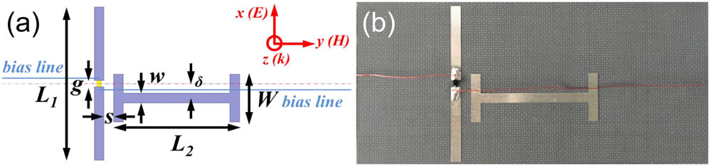
Fig. 2. (a) Simulated transmission spectra of the vertical wire alone (green curve), horizontal wire alone (blue curve), and the symmetry-broken metasurface (red curve). (b) Schematic view of destructive interference between the bright and dark modes. (c) Simulated transmission phase (blue curve) and group delay (red curve) of the symmetry-broken metasurface. (d)–(f) Distribution of the electric field on the plane where the metallic pattern is located and the induced surface current indicated by arrows on the metallic pattern at 2.97 GHz. All these results are obtained when the resistance of the PIN diode is 2 Ω.

Fig. 3. (a) Transmission spectra of the symmetry-broken metasurface predicted by the TCMT (blue points) and simulated through FEM (red curve). (b) Magnitude of the electric dipole moment of vertical wire (p v p h p 1 p 2

Fig. 4. (a) Simulated transmission spectra of the symmetry-broken metasurface and calculated magnitude spectra of p 2 δ = 0 δ

Fig. 5. (a) Measured and (b) simulated transmission spectra of the vertical wire alone on substrate with the bias voltage ranging from 0 to 1.2 V, and accordingly the resistance of the PIN diode varying from 3000 Ω to 2 Ω.

Fig. 6. Transmission spectra of the symmetry-broken metasurface obtained through both (a) experiment and (b) simulation with the bias voltage ranging from 0 to 1.2 V, and accordingly the resistance of the PIN diode varying from 3000 Ω to 2 Ω.


Ruisheng Yang, Quanhong Fu, Yuancheng Fan, Weiqi Cai, Kepeng Qiu, Weihong Zhang, Fuli Zhang. Active control of EIT-like response in a symmetry-broken metasurface with orthogonal electric dipolar resonators[J]. Photonics Research, 2019, 7(9): 09000955.


 PDF全文
PDF全文

