Mode-division multiplexing (MDM) technology has emerged as an effective solution to increase the fiber capacity in addition to the commonly used technologies, such as wavelength division multiplexing (WDM)[13" target="_self" style="display: inline;">–3], optical time division multiplexing (OTDM), polarization division multiplexing (PDM)[4,5], and advanced modulation formats. In a typical MDM system, mode conversion and multiplexing are indispensable for the transmitters, where the fundamental laser/fiber mode should be converted to high-order modes and multiplexed into a common output. Many structures have been proposed to realize mode conversion and multiplexing, which typically includes fiber-based technology[6], free-space-optics-based technology[7], and integrated-waveguide-based technology. In terms of functionality and mass-production capability, integrated waveguide technologies are promising due to their capability to be integrated with other devices on chips. Typical structures used in integrated waveguide technologies include directional couplers[8,9], adiabatic couplers[10], and multimode interference (MMI) couplers[11,12]. Due to its large fabrication tolerance and low loss, the MMI-based mode converter-multiplexer will be a potential candidate for integrated few-mode systems. In addition, as a building block for photonic integrated circuit, MMI has been widely adopted in the generic foundry model[13], enabling a high possibility of large scale integrated with active components.
The principle of MMI is based on the self-imaging effect, which can reproduce single or multiple images of the input optical field profile along the propagation of the light[14]. By choosing a proper length, width, and positions of the input and output arms of the MMI, it is possible to realize mode conversion between the fundamental mode and the first-order mode[15]. Several groups have reported the design and realization of the MMI-based mode converter/(de)multiplexer on silicon on insulator (SOI) substrate[9,11,16]. Thanks to the large wavelength tolerance of the MMI structure, the mode converter/(de)multiplexer can work in a wide wavelength range, which also indicates a possibility of WDM-compatible functionality. Considering the integration possibility of laser sources, modulators, mode converters, and wavelength-mode division multiplexers, an MDM-WDM compatible fully-integrated transmitter would be an attractive solution for future fiber communication systems. It would considerably increase the functionality and decrease the size, power consumption, and cost of such transmitters that may otherwise require a complex combination of discrete components.
In this Letter, we propose an MMI-based few-mode transmitter compatible with WDM technology. The simulation and characterization of the structure was carried out on InP substrate. The device mainly consists of lasers, modulators, and a set of MMIs for mode conversion between the fundamental mode and the first-order mode for multichannel signals, and one MMI-based wavelength-mode division multiplexer for wavelength and mode multiplexing. The choice of an MMI-based mode converter and multiplexer makes it possible to realize the mode conversion and multiplexing function through the standard design that is compatible with the generic foundry model. The choice of an InP-based material makes it possible to integrate active components to realize laser generation, modulation, and detection. The intrinsic loss of the MMI-based multiplexer can also be compensated with an optical introduction of semiconductor amplifiers or integrated laser diodes[17].
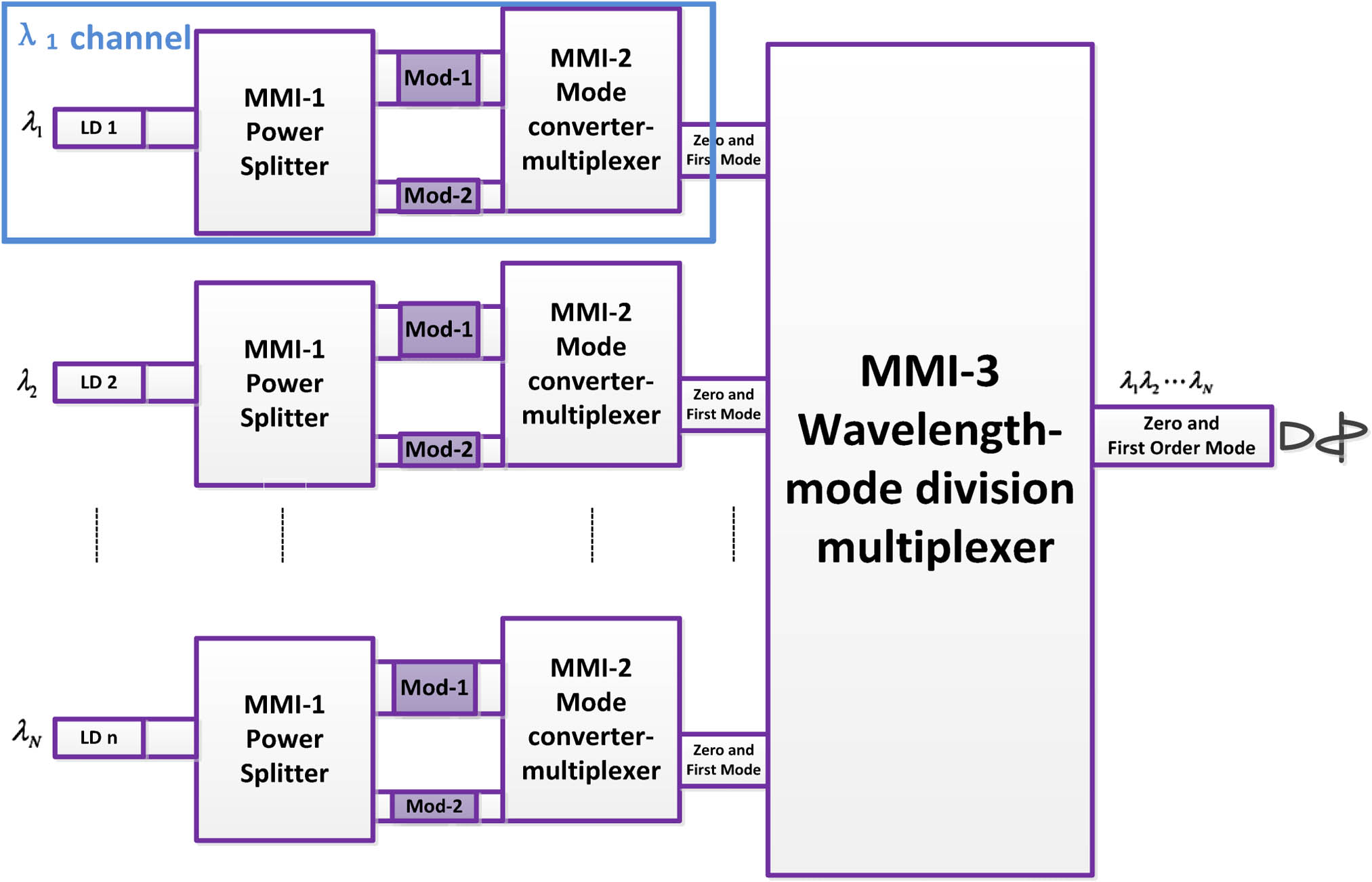
Figure 1 shows the proposed MMI-based few-mode transmitter on InP substrate. It consists of a series of laser sources, modulators, and MMIs. The laser sources can be distributed feedback (DFB) lasers or distributed Bragg reflector (DBR) lasers. The modulators can be electroabsorption (EA) modulators or Mach–Zehnder modulators. The MMIs function as the power splitters (MMI-1), mode converters/(de)multiplexers (MMI-2), and the wavelength-mode division multiplexer (MMI-3), respectively, with different design parameters. The device is designed to first realize the mode conversion/multiplexing at each wavelength, and then realize wavelength combination for different modes. Take the channel as an example, as shown in Fig. 2. The fundamental mode from laser diode is first split into two branches by a power splitter MMI-1, and then the two fundamental modes are independently modulated by modulators Mod-1 and Mod-2. The modulated signals are then sent to a mode converter/multiplexer MMI-2 where one branch of the fundamental mode is converted to the first-order mode, and combined with another branch of fundamental mode transmitted directly though the MMI-2. Finally, the multiplexed fundamental and first-order mode at are combined with modes from other channels at MMI-3 and sent out from a common port. In this design, MMI-1 is a standard MMI splitter, MMI-2 can be structures with 50%, 66%, or 100% mode conversion efficiencies[15], and MMI-3 can be structures of either a general interference MMI or a symmetric interference MMI, as shown in Fig. 3.
Fig. 1. Schematic diagram of the MMI-based few-mode transmitter.
下载图片 查看所有图片
Fig. 2. Schematic diagram of the mode converter/multiplexer.
下载图片 查看所有图片
Fig. 3. Schematic diagram of the wavelength-mode division multiplexer: (a) general interference MMI and (b) symmetric interference MMI.
下载图片 查看所有图片
The wavelength-mode division multiplexer MMI-3 is a key component in this design. Even though theoretical results predict that an MMI should be wavelength insensitive in a certain range for an arbitrary input field[18], it is still not clear whether such a structure is suitable for the combination of high-order waveguide modes at multiple wavelengths in terms of engineering manufacturability. So we verified the feasibility of a wavelength-mode division multiplexer using three-dimensional (3D) beam propagation method (BPM) simulations.
For the wavelength-mode division multiplexer MMI-3, the width of the input and output arms are set to be and , respectively. The width and length of the MMI section are denoted as and , respectively. For a general interference MMI[19], , with , where represents the number of the in- and outputs, gives multiples of the shortest MMI having outputs, represents the coupling length of the fundamental mode and the first-order mode, is the wavelength in a vacuum, is the effective width of the MMI taking into account the Goos–Hähnchen shifts, and is the effective refractive index of the ridge. The general MMI can couple any order and number of the inputs into one common output waveguide.
For a symmetric interference MMI, , where is the number of the output waveguides. The symmetric interference MMI can couple odd number of inputs with fundamental and first-order modes into one common output waveguide.
The epitaxial structure of the InP-based MMI used in the simulation is shown in Fig. 4(a). It consists of a 0.5 μm -InP buffer, a 0.3 μm InGaAsP core layer with 1.2 μm bandgap (1.2Q), and a 1 μm InP cladding whose effective indexes are 3.167, 3.382, and 3.167, respectively. The cross section view of the waveguides is shown in Fig. 4(b), where an etching depth of 1.15 μm down into the middle of the core layer is adopted to reduce excess loss[20].
Fig. 4. (a) Epitaxial structure of the MMI, and (b) the cross section view of the waveguide.
下载图片 查看所有图片
Considering the mode matching between the waveguide modes and fiber modes, the fundamental and first-order waveguide modes are normally the desired mode to be excited and multiplexed. In this case, both the general interference and the symmetric interference MMIs can be used to function as a multiplexer. To minimize the loss and device size, a () MMI structure was adopted in the simulation. The width and the length of the symmetric interference MMI were set to be 16 and 388 μm, respectively. The width of the input and output waveguides were designed to be 4 μm to support both the fundamental mode and the first-order mode.
Figures 5(a) and 5(b) show the field distributions when a fundamental mode or a first-order mode is launched into the input ports of the MMI multiplexer, respectively. As can be seen, both the fundamental and the first-order mode can exit from the common output port, suggesting a mode multiplexing function. Then the wavelength was scanned to verify the wavelength sensitivity of each mode. Figure 6 shows the calculated losses for the mode and mode, where the intrinsic loss of 4.8 dB for a MMI has been subtracted. From the figure, it can be seen that in the whole C-band, the extra losses for the mode and mode are below 0.2 and 0.8 dB, respectively.
Fig. 5. Field distributions of a symmetric interference MMI as a multiplexer (MMI-3) when (a) a fundamental mode or (b) a first-order mode is injected into a different input port.
下载图片 查看所有图片
Fig. 6. Wavelength sensitivity of the MMI wavelength-mode multiplexer when (a) the fundamental modes or (b) the first-order modes are launched from port 1 to port 3.
下载图片 查看所有图片
Then the fabrication tolerance was investigated so as to verify the feasibility of such a wavelength-mode division multiplexer. The fabrication tolerance of the MMI’s width and length were scanned at different wavelengths for both the and mode. Figure 7 shows the calculated tolerance of the length and width of the MMI. The fabrication tolerance is defined such that the deviation from the optimum device dimension will result in an extra loss below 3 dB for the two modes. From the simulations, the wavelength-mode division multiplexer was found to have a tolerance of about 30 and 0.5 μm, respectively, for the length and width direction of the MMI in the whole C-band, as shown in Fig. 7.
Fig. 7. Simulated fabrication tolerance for the (a) length and (b) width direction of the wavelength-mode division multiplexer.
下载图片 查看所有图片
Then all the contributions of MMI-1, MMI-2, and MMI-3 were calculated. The simulation was divided into two steps. The first step was to calculate the field distribution when a mode was transmitted through MMI-1 and MMI-2. The second step was to send the different modes obtained from step 1 to the wavelength-mode division multiplexer MMI-3. In the simulation, the MMI-1 was designed to have a width of 15 μm and a length of 255 μm. MMI-2 was designed to be a 66% mode converter/multiplexer, as a tradeoff between mode conversion efficiency and device size, with a width of 13 μm and a length of 510 μm. The total length of the three MMI sections was 1153 μm. The optical field distributions after the first step are shown in Figs. 8(a)–8(c). Figures 8(a) and 8(b) demonstrate the field distributions when one of the feeding arms connecting to MMI-2 is disconnected, which corresponds to a fundamental mode output and a first-order mode output, respectively. Figure 8(c) demonstrates the cases when both feeding arms are connected to MMI-2, where a mode-multiplexed pattern combing both the and mode can be observed in Output 2. The simulated field distributions after MMI-3 are shown in Figs. 8(d)–8(f) to demonstrate the cases when the multiplexed modes obtained in Output 2 are incident to the three input ports of the MMI-3, respectively. The simulated loss of the whole passive parts (MMI-1, MMI-2, and MMI-3) in the transmitter shows a maximum loss of below 0.26 dB (after subtracting the intrinsic loss of the MMIs) in the C-band, as shown in Fig. 9.
Fig. 8. Field distribution when an input mode transmits through (a–c) MMI-1 and MMI-2 and (d–e) MMI-1, MMI-2, and MMI-3. (a) and (b) are obtained by disconnecting one of the feeding arms to MMI-2.
下载图片 查看所有图片
Fig. 9. Simulated loss vs. wavelength for the whole device (the intrinsic loss of MMIs has been subtracted).
下载图片 查看所有图片
To realize the mode conversion/multiplexing of the high-order modes, the 66% mode converter/multiplexer (MMI-2) can be replaced by other designs like[21]. The wavelength-mode multiplexer (MMI-3) can also be replaced easily by the other symmetric interference MMI couplers ( being an odd number) or general interference MMI couplers ( being a positive integer) when the wavelength channel increases, where and are the number of the output waveguides.
For such an integrated device, the back reflection from the MMI couplers may influence the dynamics of the lasers, since there are no conventional isolators placed between the lasers and the MMIs. The major contribution comes from the reflection from the self-imaging point where there is no output port in which case the light at the self-image point will be reflected back into the input port and further back into the laser. A typical example is Output 2 of MMI-2, as shown in Fig. 2. When there is no actual output waveguide at Output 2, the reflectivity between the InP/InGaAsP materials and the air is about 0.3. Assuming the laser has a confinement factor of 0.05, the fraction of the laser power coupled into the laser active region will be on the order of 0.1% () after a simple arithmetic calculation. Such a back reflection level might destabilize the laser depending on the specific laser structure and material. The problem can be easily solved by introducing an absorption section at the position of Output 2. For reflections from the output ports of MMI-3, antireflection coating with a reflectivity below 1% will guarantee a feedback level well below , which can hardly destabilize the laser. Other contributions from the interface reflections between the access waveguide and the MMIs are calculated to be lower than , which can be omitted here. In real applications, MMIs with angled, rough, or absorbing end facets also can be adopted to minimize the influence of the end reflection.
In conclusion, an InP-based monolithically integrated few-mode transmitter aiming at the combination of WDM and MDM technologies is proposed by using cascaded MMI couplers. The core element of the transmitter is an MMI-based wavelength-mode division multiplexer. The performance and manufacture tolerance of the wavelength-mode division multiplexer was simulated through the 3D BPM method. Simulations show that such a multiplexer has a large fabrication tolerance of 30 and 0.5 μm, respectively, in the length and width direction, in the whole C-band wavelength range. The loss is below 0.26 dB for both the fundamental mode and first-order mode in the whole passive parts of the transmitter. This wavelength-mode division multiplexer can be integrated with other active components, capable of realizing a few-mode transmitter with WDM functionality.
Zhaosong Li, Dan Lu, Bing Zuo, Song Liang, Xuliang Zhou, Jiaoqing Pan. Proposal of an InP-based few-mode transmitter based on multimode interference couplers for wavelength division multiplexing and mode division multiplexing applications[J]. Chinese Optics Letters, 2016, 14(8): 080601.
 Download: 976次


