Photonics Research, 2016, 4 (6): 06000209, Published Online: Dec. 23, 2016  

Design of a barcode-like waveguide nanostructurefor efficient chip–fiber coupling Download: 1128次

Author Affiliations
Department of Electronic and Information Engineering, Harbin Institute of Technology, Shenzhen Graduate School, The University Town of Shenzhen, Xili, Shenzhen, China
Abstract
A barcode-like waveguide nanostructure with discretized multilevel pixel lines is designed and optimized by a nonlinear search algorithm. We obtain the design of a one-dimensional multilevel nanostructure with ?1.04 dB efficiency for surface normal coupling to a standard single-mode fiber. Another design is achieved from the automatic optimization process, which enables polarization-independent coupling to a single-mode fiber. The optimum coupling efficiency is simulated to be ?2.83 dB for TE and ?3.49 for TM polarization centered near the 1550 nm wavelength. Polarization-dependent loss of less than 1 dB over 45.3 nm is achieved.

1. INTRODUCTION

A grating coupler is an enabling technique for the input–output (I/O) of chip scale interconnection [13]. Because of distinct advantages over other material systems, silicon photonics is a proven platform for optical interconnects. However, because the large refractive index contrast of optical waveguides fabricated on silicon-on-insulator (SOI), a huge mode field size mismatch exists between the fiber and the silicon submicrometer waveguide. Butt coupling with an inversed taper [4,5] or a grating taper [6] could be used to interface the optical fiber and the submicrometer sized waveguide, but this requires facet polishing and is not compatible with wafer scope testing. A grating coupler is another option that has been shown to be an efficient light coupling technique in silicon photonics [79].

Several practical issues arise before grating coupler can be implemented as the I/O solution. In particular, a grating coupler with vertical light diffraction is desired as it has smaller packaging difficulties compared with off-normal fiber coupling. However, this type of grating suffers from second-order Bragg reflection, which limits coupling efficiency. To overcome this limit, a slant grating structure [10], a chirped grating [11], and a quasi-periodic multiple slot grating [12] were used to suppress the backreflection. However, a periodic grating structure with one or two etching steps is normally designed based on first principles with limited degrees of freedom, and it consumes much operational expenses. In addition, the manual design becomes complicated if more etching steps are allowed due to fabrication advances. Hence, it would be beneficial if nanophotonic devices could be designed by algorithm. In [12], a genetic algorithm was used by Covey and Chen to demonstrate a grating coupler, but with a dual layer horizontal slot waveguide structure, which is not standard for photonic integrated circuits. Piggott et al. demonstrated a wavelength division multiplexing (WDM) grating using objective-first design [13], but the efficiency is not high and the fiber–chip coupling scenario is not considered.

Another issue with silicon grating couplers is the polarization dependence. There has been much work reported to realize a polarization independent or insensitive grating coupler. Two-dimensional (2D) polarization diversity circuits were used, but this doubles the chip area [14,15]. Subwavelength structures balancing the effective index between TE and TM were also proposed to achieve polarization independence [16,17]. More recently, a tapered grating nanostructure was demonstrated to achieve polarization-insensitive coupling [6]. However, they all require an elaborate design process. Because of the large index difference for TE and TM, a polarization-insensitive grating coupler is much more difficult to design than is a single-polarization case. Thus. developing an automatic design approach becomes more important.

In this paper, we utilized a modified direct binary search algorithm to automatically design a barcode-like one-dimensional (1D) nanostructure for chip–fiber coupling. A QR-code-like 2D subwavelength nanostructure designed by algorithm has been demonstrated as an ultracompact polarization beam splitter [18], wavelength multiplexer [19], and for waveguide bending [20]. Here we show that a discretized waveguide nanostructure could be designed by algorithm for different functionalities. We obtain two structures, with one for chip surface normal coupling to a vertically located fiber and the other for polarization-independent coupling.

2. OPTIMIZATION PROCESS

A conventional periodic grating coupler is normally fabricated with no more than two etching steps. The designer must carefully optimize the fill factor and the grating period to minimize the backreflection and match the coupling strength with the fiber mode profile.

Here we introduce a modified direct search algorithm to automatically design a diffractive nanostructure for chip–fiber coupling. We consider an SOI substrate with 340 nm top silicon and 3 μm buried oxide (BOX). The coupling area was discretized equally into 125 pixel lines along the light propagation direction, and each line is a narrow slab with 120 nm width. The narrow silicon slab thickness is divided equally into four- and eight-level heights of the total 340 nm top silicon, similar to the digital multilevel modulation formats. Therefore, the effective index of each slit can be engineered with more flexibility by choosing different thicknesses. A side-view schematic of the proposed nanostructure is shown in Fig. 1. The design process begins with a random seed of initial parameters that includes the thickness of each slit so that the nanostructure is initialized with a string of 125 random numbers. Then we randomly change the slit thickness level one by one along the light propagation direction and the figures of merit (FOMs) are numerically simulated by the 2D finite difference time domain (FDTD) method. In each iteration, the randomly changed slit thickness level will be effective if the FOM is found to be improved. The convergence radius is dynamically adjusted according to the feedback from the simulation. It finally converges to the objective via a certain number of iterations. The detail convergence condition will be illustrated in the following sections for different cases.

Fig. 1. Side-view schematic of the proposed discretized nanostructure.

下载图片 查看所有图片

3. RESULTS AND DISCUSSION

3.1 A. Vertical Coupling Nanostructure Design

First we investigate the possibility of getting a surface normal coupling design using a computer-optimized barcode-like nanostructure. We first define a random nanostructure to initialize the design process. The optimization process iterates based on the modified direct search algorithm described above. The FOM we are interested in here is coupling efficiency, which is calculated by taking the overlap between the fiber mode field and the diffraction field into account. The convergence radius ρi decreases monotonically when the FOM is larger in the ith iteration. When the better parameters have been found, the FOM becomes closer to the objective. We need to point out that we could set multiple objectives, such as coupling efficiency, diffraction angle, bandwidth, and other FOMs. The convergence condition can be expressed as |FOMi+1FOMu1|>ρi.

On the other hand, the more levels we define, the more freedom we have to optimize the diffraction structure. From the standpoint of fabrication, it would be challenging to use more than two etching steps, but the focusing ion beam writer could be a promising option to fabricate such multilevel nanostructures [21].

We use a 4-core standard desktop computer operating at 4 GHz. The design process of the nanostructure with vertical coupling is completed within 72 h. The side view of the optimized nanostructure schematic is shown in Figs. 2(a) and 2(b) for four-level and eight-level structures, respectively. We observed 120 slits (pixels) with different thicknesses and, hence, different effective indices. The color bars shown in Figs. 2(c) and 2(d) represent the optimized effective indices of the discretized grating lines with different levels along the light propagation direction. It should be noted that the effective index is higher when the thickness is larger. The effective indices at different levels varies from 1.5 to 3.1, which provides design flexibility.
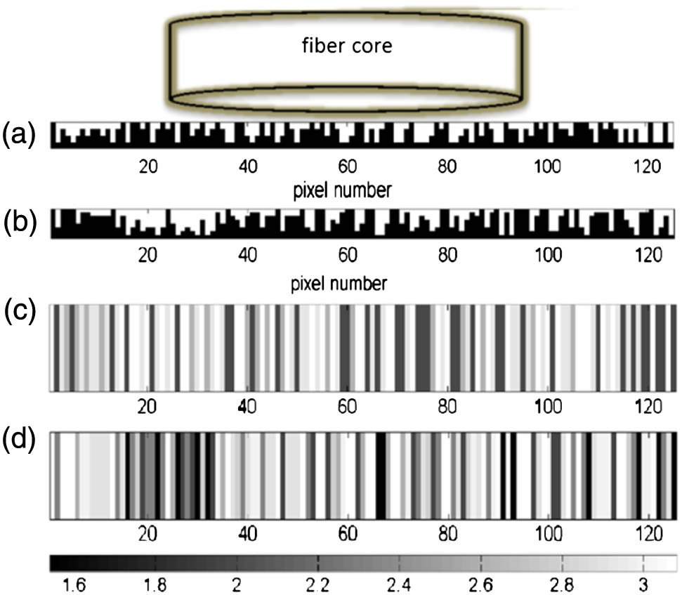
Fig. 2. Side-view schematics of the optimized coupling nanostructures for (a) four levels and (b) eight levels. Gray-scale representations of the discretized effective indices of the (c) four-level and (d) eight-level vertical coupling nanostructures.

下载图片 查看所有图片

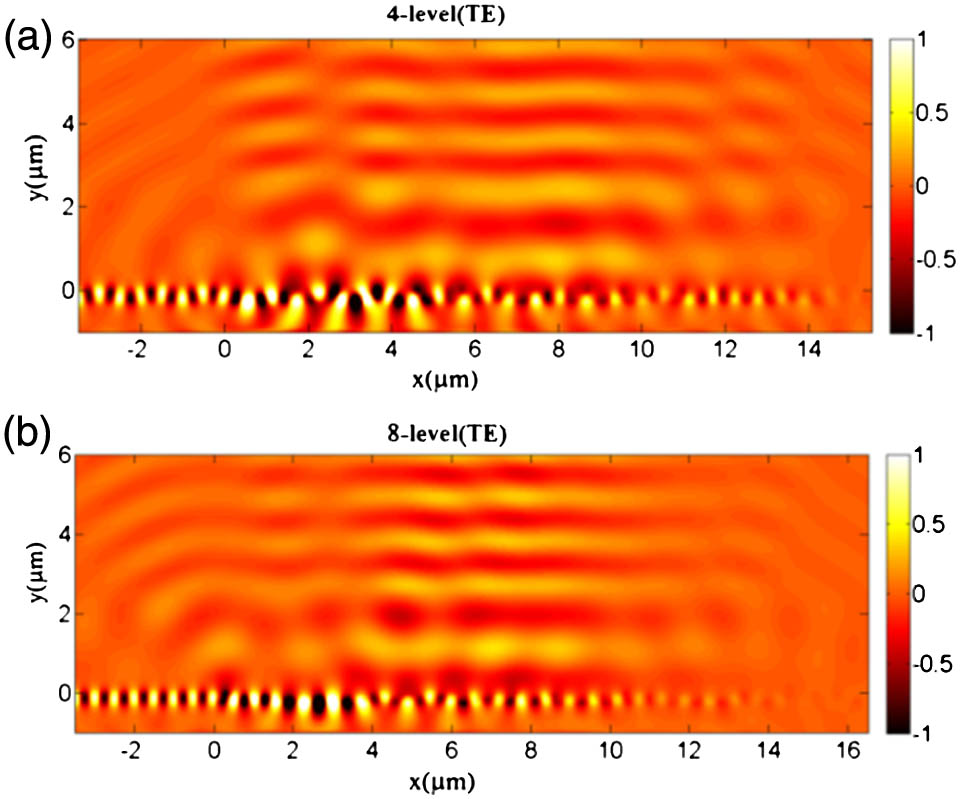
During the FDTD simulation, we set a power monitor at the bottom of the BOX layer, and the obtained value indicates that the leakage into the substrate is quite small, as shown in Fig. 3(a). Thus, the optimized structure has good control of the constructive interference between the upward wave from the grating tooth and the interface between the BOX and the silicon substrate. Hence a good directionality is achieved, as well. One of the advantages of this type of structure is that the backreflection is naturally suppressed without angle tilt alignment. The results depicted in Fig. 3(b) show that the reflection around 1550 nm has been optimized at a low level, which allows for a high coupling efficiency. Because the eight-level structure has more degrees of design freedom, it suppresses the reflection to a much lower level than the four-level structure. After optimization, the light can be coupled to the optical fiber with an efficiency of 2.51  dB for the four-level and approximately 1.04  dB for the eight-level grating coupler, which is shown in Fig. 3(c). To confirm the validity of 2D FDTD, we calculate the coupling efficiency of the optimum eight-level structure using three-dimensional (3D) FDTD. The coupling efficiency is approximately 1.54  dB, which is slightly lower than the 2D calculation. The coupling efficiency is calculated considering the overlap of the diffractive light beam and the mode profile of a standard single-mode fiber for the 1550 nm wavelength. The 3 dB bandwidths of the proposed structures are 30 and 40 nm for the eight- and four-level structures, respectively. The simulated mode fields diffracted from the optimized structures with four and eight levels are shown in Figs. 4(a) and 4(b), respectively. The light diffraction angle is observed to be zero to the structure surface normal. To investigate the fabrication tolerance of this device, we have considered ±10  nm thickness variation of each slab line due to fabrication error. The optimum coupling efficiency drops 20% for the eight-level structure and 5% for the four-level structure.
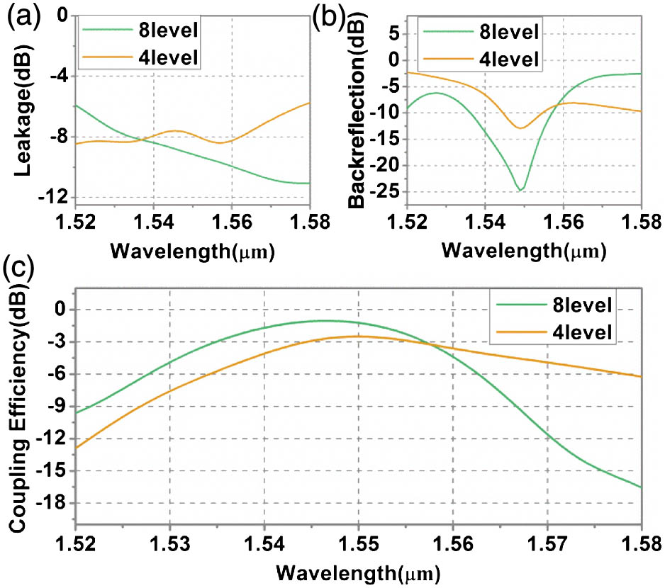
Fig. 3. (a) Simulated amount of light leakage to the substrate. (b) Backreflection of the designed nanostructure. (c) Coupling efficiency of the two types of nanostructure.
下载图片 查看所有图片

Fig. 4. Simulated optical field distribution of the diffracted wave for the (a) four-level and (b) eight-level nanostructures, respectively.

下载图片 查看所有图片

3.2 B. Polarization-Independent Nanostructure Design

In addition to the coupling angle, polarization dependence is another tough issue for a high index contrast grating coupler. Here we propose to optimize the diffractive nanostructure to achieve polarization independence. For a polarization-insensitive nanostructure, we have to define two output objectives, which are the coupling efficiencies for the quasi-TE and quasi-TM waveguide modes. Thus, it becomes a multiple objective problem, and the general convergence condition for such problem can be expressed as (jηj,i+1jηj,i>1)[(|ηj+1,iηj,i1|)<ρi],where ηj,i is the ith iterating FOM of the jth output objective (j=1 for TE and j=2 for TM) in this case. The ith radius of convergence ρi dynamically varies in relation to the simulation feedback and comes to zero after a certain number of iterations. It could be expressed as ρi=f(jηj,i1),where f(x) is a decreasing function that relates to the iteration error and computing time. It should be noted that we could change the sign of the second-order derivative of f(x) to relax or tighten the convergent condition.

The entire design consumes about 144 h using the same desktop as we described before. The optimized structure schematic for polarization-independent coupling is shown in Fig. 5(a). The corresponding effective indices are calculated and are shown in Figs. 5(b) and 5(c) for TM and TE light, respectively.
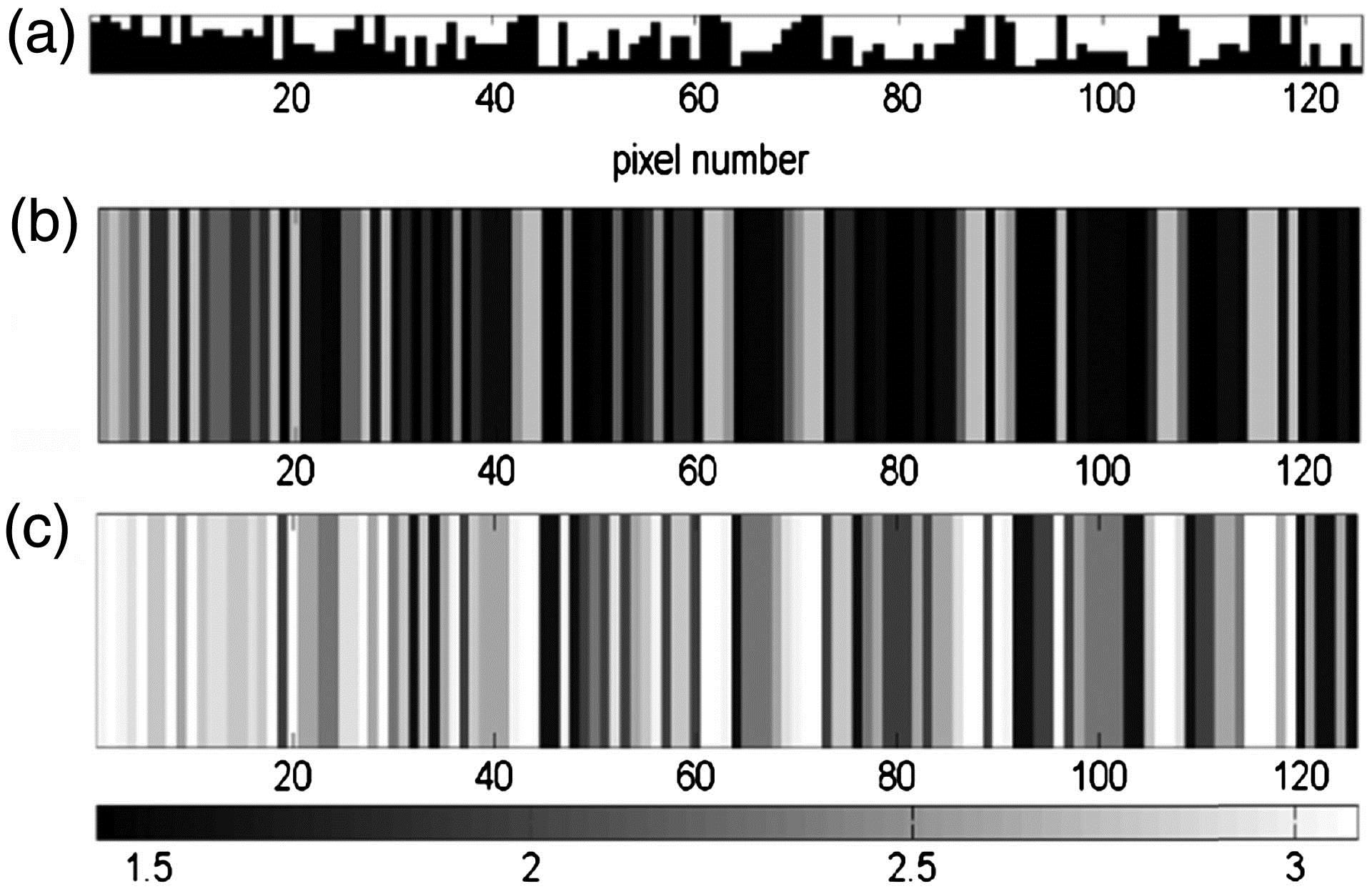
Fig. 5. (a) Side-view schematic of the optimized eight-level polarization-independent nanostructure. Gray-scale representations of the discretized effective indices of the optimized structure for (b) TM and (c) TE.

下载图片 查看所有图片

The light diffracted toward the substrate is monitored in the simulation and the results are plotted in Fig. 6(a). The leakage is maintained at approximately 6  dB for TE and even lower for TM. The backreflection from structure to waveguide is also considered and shown in Fig. 6(b). From the backreflection curves, we can see that the backreflections for both the TE and TM mode are close to 0 at wavelengths near 1550 nm. Thus, the algorithm suppresses the backreflection to a low level. The coupling efficiencies of the TE and TM polarizations are shown in Fig. 6(c); they are 2.83 and 3.49  dB, respectively. The 3 dB bandwidths of TE and TM modes are 55 and 95 nm, respectively. The polarization-dependent loss (PDL) is indicated by the dashed line in Fig. 6(c). The span for PDL within 1 dB is around 45.3 nm. The optical bandwidth of the diffractive structure is determined by several factors, including structure effective index and dispersion. The trade-off between coupling efficiency and the PDL could be more balanced, but more calculation time is needed. We also investigate the discrepancy between the 2D and 3D FDTD. The coupling efficiency of the optimum polarization-independent eight-level structure simulated by 3D FDTD is 3.2  dB for TE and 3.89  dB for TM.
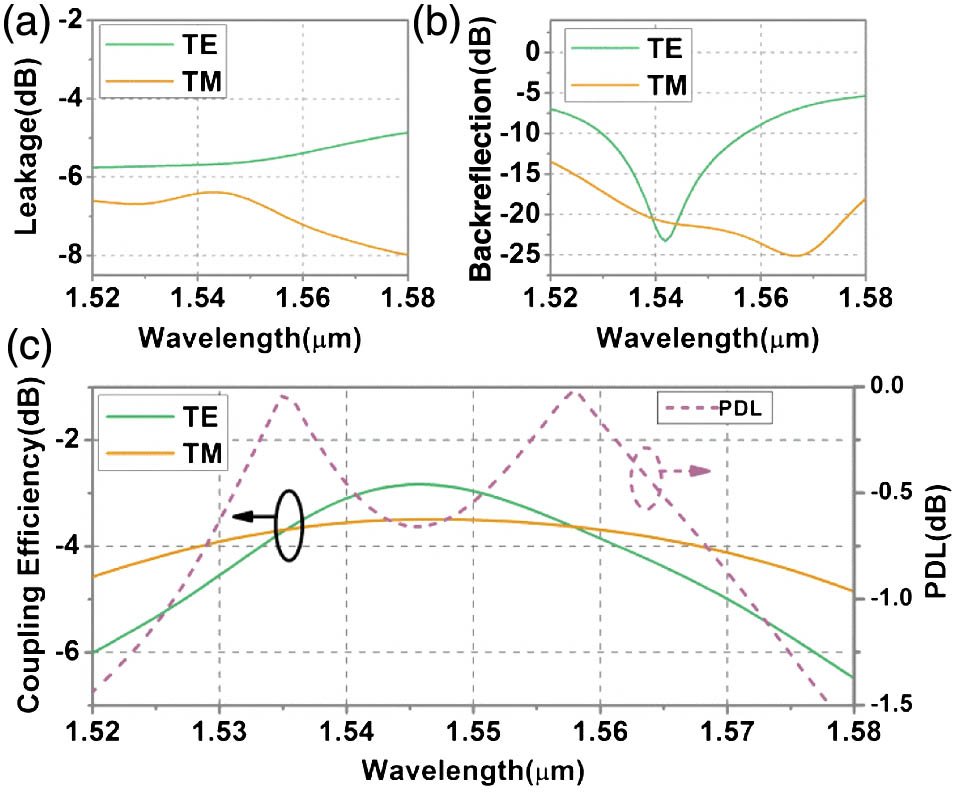
Fig. 6. (a) Simulated amount of light leakage to the substrate. (b) Backreflections of the TE and TM modes from structure to waveguide. (c) Coupling efficiencies of the TE- and TM-mode light coupling from waveguide to single-mode fiber in the polarization-independent nanostructure.

下载图片 查看所有图片

The simulated field distribution of light diffraction from the optimized eight-level grating coupler is shown in Fig. 7(a) for TE and Fig. 7(b) for TM polarization. We observe a strong optical wave coupled from the structure into the single-mode fiber with 10° coupling angle with respect to the surface normal. The field intensity is quite similar for TE and TM. The coupling efficiency could be further improved if the pixel is chosen to be smaller, but it would be more challenging to fabricate. Bandwidth control could also be achieved if we set another output objective, thus increasing computing complexity.
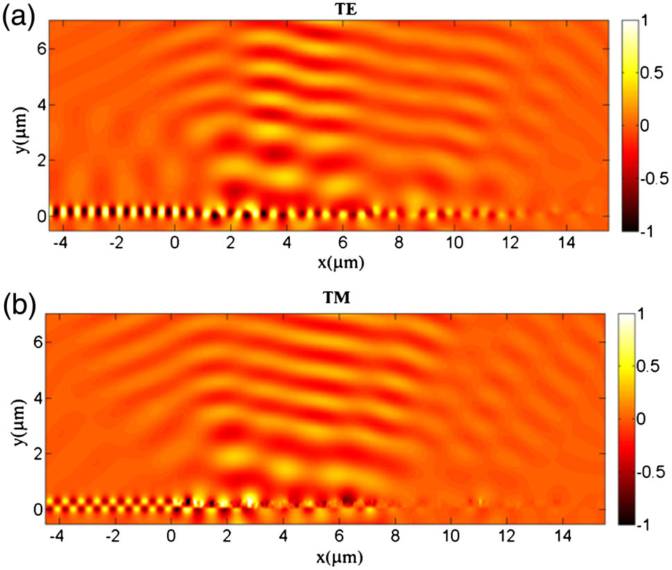
Fig. 7. Diffractive electric field of the eight-level structure for (a) TE and (b) TM polarization.

下载图片 查看所有图片

4. CONCLUSION

We have proposed a barcode-like 1D nanostructure for chip–fiber coupling using a modified direct search algorithm. We have addressed the coupling angle and the polarization issue, both of which are difficult to address in a periodic grating. The algorithm can be regarded as a general method to design a coupling nanostructure with multiple objectives, such as bandwidth, coupling efficiency, polarization, and coupling angle. A nanostructure with surface normal diffraction is achieved, and the efficiency is as high as 1.04  dB. The polarization-independent coupling efficiency is also achieved to be less than 3.5 dB, and the PDL is less than 1 dB over a 45.3 nm wavelength range.

References

[1] J. Song, X. Luo, X. Tu, L. Jia, Q. Fang, T. Liow, M. Yu, G. Q. Lo. Three-dimensional (3D) monolithically integrated photodetector and WDM receiver based on bulk silicon wafer. Opt. Express, 2014, 22: 19546-19554.

[2] K. Xu, L. G. Yang, J. Y. Sung, Y. M. Chen, Z. Z. Cheng, C. W. Chow, C. H. Yeh, H. K. Tsang. Compatibility of silicon Mach–Zehnder modulators for advanced modulation formats. IEEE J. Lightwave Technol., 2013, 31: 1170-1177.

[3] K. Xu, Z. Cheng, C. Y. Wong, H. K. Tsang. Tunable integrated variable bit-rate DPSK silicon receiver. Opt. Lett., 2012, 37: 4738-4740.

[4] V. R. Almeida, R. R. Panepucci, M. Lipson. Nanotaper for compact mode conversion. Opt. Lett., 2003, 28: 1302-1304.

[5] G. Ren, S. Chen, Y. Cheng, Y. Zhai. Study on inverse taper based mode transformer for low loss coupling between silicon wire waveguide and lensed fiber. Opt. Commun., 2010, 284: 4782-4788.

[6] P. Cheben, J. H. Schmid, S. Wang, D.-X. Xu, M. Vachon, S. Janz, J. Lapointe, Y. Painchaud, M. J. Picard. Broadband polarization independent nanophotonic coupler for silicon waveguides with ultra-high efficiency. Opt. Express, 2015, 23: 22553-22563.

[7] F. V. Laere, T. Claes, J. Schrauwen, S. Scheerlinck, W. Bogaerts, D. Taillaert, L. O. Faolain, D. V. Thourhout, R. Baets. Compact focusing grating couplers for silicon-on-insulator integrated circuits. IEEE Photon. Technol. Lett., 2007, 19: 1919-1921.

[8] X. Chen, C. Li, C. K. Y. Fung, S. M. G. Lo, H. K. Tsang. Apodized waveguide grating couplers for efficient coupling to optical fibers. IEEE Photon. Technol. Lett., 2010, 22: 1156-1158.

[9] Z. Cheng, X. Chen, C. Y. Wong, K. Xu, H. K. Tsang. Broadband focusing grating couplers for suspended-membrane waveguides. Opt. Lett., 2012, 37: 5181-5183.

[10] B. Wang, J. H. Jiang, G. P. Nordin. Embedded slanted grating for vertical coupling between fibers and silicon-on-insulator planar waveguides. IEEE Photon. Technol. Lett., 2005, 17: 1884-1886.

[11] X. Chen, C. Li, H. K. Tsang. Fabrication-tolerant waveguide chirped grating coupler for coupling to a perfectly vertical optical fiber. IEEE Photon. Technol. Lett., 2008, 20: 1914-1916.

[12] J. Covey, R. T. Chen. Efficient perfectly vertical fiber-to-chip grating coupler for silicon horizontal multiple slot waveguides. Opt. Express, 2013, 21: 10886-10896.

[13] A. Y. Piggott, J. Lu, T. M. Babinec, K. G. Lagoudakis, J. Petykiewicz, J. Vuckovic. Inverse design and implementation of a wavelength demultiplexing grating coupler. Sci. Rep., 2014, 4: 7210.

[14] X. Chen, C. Li, H. K. Tsang. Two dimensional silicon waveguide chirped grating couplers for vertical optical fibers original research article. Opt. Commun., 2010, 283: 2146-2149.

[15] M. Streshinsky, R. Shi, A. Novack, R. T. P. Cher, A. E. J. Lim, P. G. Q. Luo, T. B. Jones, M. Hochberg. A compact bi-wavelength polarization splitting grating coupler fabricated in a 220 nm SOI platform. Opt. Express, 2013, 21: 31019-31028.

[16] X. Chen, H. K. Tsang. Polarization-independent grating couplers for silicon-on-insulator nanophotonic waveguides. Opt. Lett., 2011, 36: 796-798.

[17] Z. Cheng, H. K. Tsang. Experimental demonstration of polarization-insensitive air-cladding grating couplers for silicon-on-insulator waveguides. Opt. Lett., 2014, 39: 2206-2209.

[18] B. Shen, P. Wang, R. Polson, R. Menon. An integrated-nanophotonics polarization beamsplitter with 2.4 μm × 2.4 μm footprint. Nat. Photonics, 2015, 9: 378-382.

[19] A. Y. Piggott, J. Lu, K. G. Lagoudakis, J. Petykiewicz, T. M. Babinec, J. Vuckovic. Inverse design and demonstration of a compact and broadband on-chip wavelength demultiplexer. Nat. Photonics, 2015, 9: 374-377.

[20] B. Shen, R. Polson, R. Menon. Metamaterial-waveguide bends with effective bend radius < λ0/2. Opt. Lett., 2015, 40: 5750-5753.

[21] B. Shen, P. Wang, R. Polson, R. Menon. Ultra-high-efficiency metamaterial polarizer. Optica, 2014, 1: 356-360.

Xiang Wen, Ke Xu, Qinghai Song. Design of a barcode-like waveguide nanostructurefor efficient chip–fiber coupling[J]. Photonics Research, 2016, 4(6): 06000209.

引用该论文: TXT   |   EndNote

相关论文

加载中...

关于本站 Cookie 的使用提示

中国光学期刊网使用基于 cookie 的技术来更好地为您提供各项服务,点击此处了解我们的隐私策略。 如您需继续使用本网站,请您授权我们使用本地 cookie 来保存部分信息。
全站搜索
您最值得信赖的光电行业旗舰网络服务平台!