1 024×1 024 AlGaN紫外焦平面读出电路的超低功耗设计
Design of ultra-low-power readout circuit for 1 024×1 024 UV AlGaN focal plane arrays
1 中国科学院上海技术物理研究所 传感技术联合国家重点实验室,上海 200083
2 中国科学院上海技术物理研究所 红外成像材料与器件重点实验室,上海 200083
图 & 表
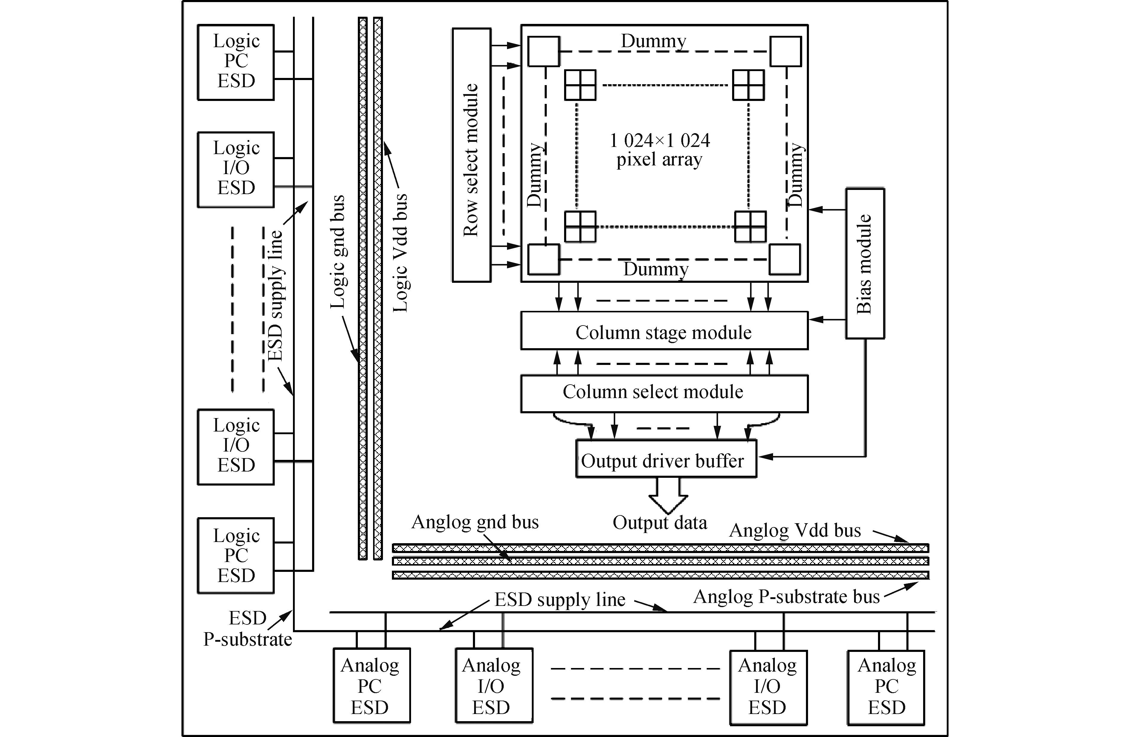
图 1.
Fig. 1. System architecture for UV AlGaN FPA readout circuit with whole chip ESD protection
下载图片 查看原文
图 2.
Fig. 2. Pixel arrays and column level circuits
下载图片 查看原文
图 3.
Fig. 3. Design of column buffer circuit
下载图片 查看原文
图 4.
Fig. 4. Architecture of whole chip bias supply
下载图片 查看原文
图 5.
Fig. 5. Die photograph of ROIC chip
下载图片 查看原文
图 6.
Fig. 6. Test platform of the ROIC chip and test result
下载图片 查看原文
图 7.
Fig. 7. Measurement results of 1 024×1 024 ROIC with eight outputs by acquisition card
下载图片 查看原文
表 1Comparision of power consumption
Table1. Comparision of power consumption
| Parameter | Previous[11] | This paper | | Array format | 128×128 | 1 024×1 024 | | Pixel current/nA | 499 | 8.5 | | Total power consumption/mW | 49.2 | 67.3 |
|
查看原文
表 2ROIC of UVFPA specifications
Table2. ROIC of UVFPA specifications
| Parameter | Measurement | | Array format | 1 024×1 024 | | Pixel size | 18 µm×18 µm | | Operate mode | Snapshot | | Pixel current/nA | 8.5 | | Power consumption | 67.3 mW @2 MHz | | Frame rate | 15 Hz(limited by speed of acquisition card) | | Integration capacitor Charge capacity | 0.11 Me- at 10 fF &1.23 M e- at 110 fF
| | Output swing/V | 1.8 | | Power supply/V | 3.3 | | Chip area | 19.30 mm×20.17 mm |
|
查看原文
谢晶, 李晓娟, 张燕, 李向阳. 1 024×1 024 AlGaN紫外焦平面读出电路的超低功耗设计[J]. 红外与激光工程, 2020, 49(5): 20190491. Xie Jing, Li Xiaojuan, Zhang Yan, Li Xiangyang. Design of ultra-low-power readout circuit for 1 024×1 024 UV AlGaN focal plane arrays[J]. Infrared and Laser Engineering, 2020, 49(5): 20190491.


 PDF全文
PDF全文
