1. INTRODUCTION
Manipulating light at a subwavelength level is the cornerstone for many optical applications, such as compact photonic devices and all-optical chips. This demand has driven the rapid development of metamaterials comprising arrayed artificial atoms. Although having exotic properties and wide applications, most of the metamaterials still remain at the laboratory stage. One of the main limitations is the significant ohmic loss associated with plasma resonances in conventional metamaterials, limiting their efficiency for a wide range of applications. Thus, reducing this loss is essential for highly efficient photonic devices. Recently, it was demonstrated that limitations could be addressed by using high-index dielectric resonators, because dielectric resonances are induced by displacement current rather than conduction current. Over the past several years, all-dielectric metamaterials have been investigated to exhibit various novel properties, including zero index [1], optical magnetism [2], local field enhancement [35" target="_self" style="display: inline;">–5], and directional scattering [6], which highlight a wide variety of applications in wavefront control [7–12" target="_self" style="display: inline;">–12], sensing [13,14], surface-enhanced spectroscopy [15], reflectors [1618" target="_self" style="display: inline;">–18], and absorbers [19].
Whereas all-dielectric metamaterials have become a hotbed of research, ranging from the infrared to optical regions, they are seldom reported in the terahertz range, which is an important spectral region that has wide applications in wireless communication, sensing, security, and chemical identification. This is different from those made of metallic structures, which have been widely reported in terahertz ranges [20–31" target="_self" style="display: inline;">–31]. One of the main limitations is the high cost of fabrication techniques. Over the past few years, attempts have been made to obtain terahertz all-dielectric metamaterials. There are three methods: direct laser patterning, deep etching, and a chemical method. The direct laser-patterning method has proven to be a high-precision and material-free fabrication approach to all-dielectric metamaterials [32,33]. However, this method suffers from expensive fabrication, inevitably blurred boundaries, and complex thickness reduction processes. Using deep-etching methods, silicon-based all-dielectric metamaterials in the terahertz range have been demonstrated in several studies [34–37" target="_self" style="display: inline;">–37]. Whereas these metamaterials show high-precision patterns and high-quality Mie resonances, reducing the high fabrication costs remains an immense challenge. Recently, a cost-effective method was reported, based on high-throughput titanium dioxide spherical resonators using a chemical method. However, the resonators are difficult to assemble, and applications were impeded in some cases [38]. Clearly, the above fabrication methods have difficulty in achieving a good balance between precision and cost.
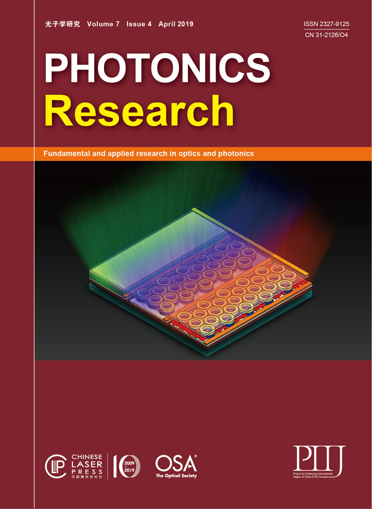
In this work, inspired by the template-assisted self-assembly method, we address this limitation by developing a novel approach, called the micro-template-assisted self-assembly (MTAS) method. We demonstrate that this method is capable of fabricating ultra-large-scale, high-precision, and flexible ceramic microsphere all-dielectric metamaterials with an area exceeding . Additionally, by using proper templates, the ceramic microsphere resonators can be readily assembled into nearly any arrangement, including complex aggregates. Next, the all-dielectric metamaterial is prepared on an active material, with which the microsphere resonators can be assembled into closely packed metasurfaces under heat treatment (HT), leading to a broadband reflector with a bandwidth of 0.15 THz and a reflection up to 95%. This work provides a versatile and powerful platform for terahertz all-dielectric metamaterials, which should find a wide variety of applications in low-loss and highly efficient terahertz devices.
2. METHOD
Before introducing the MTAS method, the nano-template-assisted self-assembly (NTSA) method is illustrated in Fig. 1(a) for comparison [39]. The fundamental process for this technology includes several steps. First, a template with holes or other patterns is fabricated and mounted on a motorized stage. A droplet of particles, usually a concentrated monodispersed solution, is sandwiched between the template and a fixed glass slide. Then, the template is slowly moved relatively to the slide, drawing the droplet meniscus across the template. When the meniscus moves over the holes, nanoparticles at the template–meniscus interface are pushed into the holes and are assembled by using capillary and gravity forces. Based on this process, by choosing appropriate templates and nanoparticles, complex aggregates of nanoparticles with well-defined shapes, sizes, and structures can be readily obtained.
Fig. 1. Illustrations of the (a) NTSA [39] and (b) MTAS methods.
下载图片 查看所有图片
Inspired by NTSA technology, we developed the MTAS method, illustrated in Fig. 1(b). This method requires only a few steps. First, a template with the desired geometry is attached to the target substrate. Then, the microspheres are placed on the template. A soft slicker is employed to blow the microspheres from left to right. The microspheres are pushed into the holes and assembled with external forces () and gravity (). Here, functions as the capillary force in the NTSA method. Note that when using the NTSA method, the nanoparticles can be in physical contact because of the attractive capillary force caused by solvent evaporation. To fix the microspheres, a thin adhesive layer is employed between the template and target substrate. Finally, the template is removed and a well-controlled microsphere-based all-dielectric metamaterial is obtained.
In the fabrication, the stainless steel membrane template is fabricated by a solid-state laser (Enpon-Nano-H532, a nanosecond laser), which has a work wavelength, output power, and pulse duration of 532 nm, 7 W, and 10 ns, respectively. First, the stainless steel membrane with a thickness of 150 μm is placed on the workbench. Holes with various geometries are etched with proper AutoCAD files. The measured terahertz transmission spectra are obtained by using the photoconductive switch-based terahertz time-domain spectroscopy. The reflection of the fabricated sample is achieved by using terahertz spectroscopic/imaging system TAS7500SL, ADVANTEST.
3. RESULTS AND DISCUSSION
To demonstrate its capability and feasibility, we fabricated a single-layer -based all-dielectric metamaterial on a flexible substrate. The micro- ceramic spheres were prepared according to our previous work [40]. Here, smooth, uniform, and spherical ceramic spheres with a diameter of were employed. In the experiment, a 50-μm-thick polyimide (PI) film was used as a substrate, because of its low permittivity () and low loss () in the terahertz range. To obtain an adhesive layer, 2-μm-thick glue was cast on the PI film. A 150-μm-thick stainless steel membrane with micro through-holes () was chosen as the template, and attached to the adhesive layer. The stainless steel membrane template was fabricated by laser etching, which ensures high precision and low cost. To assemble the microspheres on the substrate, they were placed on one side of the template. A slicker, used in screen printing, was employed to softly blow the microspheres from the left to the right. Using an appropriate strength, single-layer spheres were pushed into the holes and firmly attached to the substrate. Then, the template was carefully peeled off, and a single-layer all-dielectric metamaterial was obtained.
In this method, no organic solvents, vacuum, or complex equipment are required, ensuring low-cost and environmentally friendly fabrication. Additionally, this method is fast and effective. The microscope image of the fabricated sample is shown in Fig. 2(a), where micro ceramic spheres are highly arrayed on the substrate. Thus, a single-layer all-dielectric metamaterial, based on micro ceramic spheres is obtained. Because the arrangement of the ceramic spheres is highly dependent on the stainless steel membrane template, one can prepare metamaterials with the desired structures using proper templates. Furthermore, this method is a generic way that can be extended to other terahertz all-dielectric metamaterials based on microspheres. To confirm these two advantages, an microsphere-based all-dielectric metamaterial was prepared with this method. microspheres with a diameter of 80 μm were employed, whereas the template had holes of diameter 85 μm and a lattice constant () of 200 μm. The fabricated metamaterial sample is shown in Fig. 2(b), where uniform microspheres are arrayed on the substrate with the desired arrangement. In this method, the fabricated area is also dependent on the area of the employed template. By using a large-scale template, one can obtain an ultra-large-scale metamaterial, which is highly desirable in practical applications. In the experiment, a 90-mesh sieve with a diameter of 40 cm was utilized. By using the MTAS method, we fabricated an ultra-large-scale and rolled metamaterial with an area exceeding [Figs. 2(c) and 2(d)]. This sample, to the best of our knowledge, is the largest all-dielectric metamaterial operating in the terahertz range. It should be noted that large-scale metallic metamaterials in the terahertz range have been reported [41,42]. However, large-scale all-dielectric metamaterials are rarely found.
Fig. 2. Microscope images of the fabricated (a) and (b) all-dielectric metamaterials. Photographs of (c) the fabrication process and (d) the fabricated ultra-large-scale flexible all-dielectric metamaterial using the MTAS method. (e) Simulated and measured transmissions for and all-dielectric metamaterials. The insets are simulated magnetic field intensity distributions at the corresponding resonance dips in the H–k plane.
下载图片 查看所有图片
The resonances can be predicted by using Mie theory. Here, a nonmagnetic sphere with relative permittivity , relative permeability , and radius , in air or vacuum (), is applied. The first magnetic resonance (namely, the magnetic dipole) is considered. According to Wheeler et al. [43], the magnetic dipole portion of the scattered field is proportional to where , , , and are the Riccati–Bessel functions. By equating the denominator of this equation to zero and employing the long-wavelength condition, one can obtain the first magnetic resonance (), approximatively where is the velocity of light in vacuum. The permittivity and loss of the ceramic spheres were 35.0 and 0.01, whereas those for were 10.0 and 0.01, respectively. By applying this equation to the and metamaterials, one can obtain the first magnetic resonances at frequencies of 0.337 and 1.181 THz, respectively.
Using a terahertz time-domain spectroscopy system, the corresponding transmission spectra for the above samples were measured [Fig. 2(e)]. Regarding the ceramic sphere all-dielectric metamaterial, two remarkable resonance dips were observed at 0.366 and 0.509 THz. In the sphere all-dielectric metamaterial, the first two resonance dips were observed at 1.228 and 1.333 THz. Compared to the all-dielectric metamaterial, the resonances of the all-dielectric metamaterial shift to higher frequencies due to the lower permittivity and smaller size of spheres. It can be found that the theoretical predictions for the magnetic resonances are in good coincidence with experimental results. The deviation can be explained in two ways. First, in the theory prediction, the substrate has not been considered. Second, the permittivity in the experiment is frequency dependent. Simulations based on CST Microwave Studio (commercial software) were also conducted to obtain the transmission spectrum. In the simulation, unit cell boundary conditions are employed. Good agreement can be observed between the simulation and experimental results, confirming the high quality of the fabricated samples. It should be noted that the measured resonances have a lower -factor value, which is associated with the deviation of the sphere diameter and placing locations.
To further demonstrate the robustness of this method, we assembled these microspheres into a variety of complex meta-aggregates, such as touching dimers, trimers, quadrumers, and chains, which are difficult or impossible to obtain with other approaches. These meta-aggregates are of great interest, because they exhibit many unique properties, which would find plenty of applications. For example, the all-dielectric dimer generates a remarkable electric-field enhancement between two resonators; this can be applied to high surface-enhanced fluorescence and surface-enhanced Raman scattering [44]. Meanwhile, the touching all-dielectric trimer has been demonstrated to support electromagnetically induced transparency [45], whereas the all-dielectric trimer can produce a new type of Fano resonance [46]. However, this meta-aggregate seems difficult to obtain by using conventional methods. In fact, this limitation can be addressed by adjusting the shape and dimensions of the templates. In the experiment, the touching dimer, trimer, quadrumer, and chain were obtained by using proper templates [Figs. 3(a)–3(d)]. Here, the holes should be just larger than the meta-aggregates. This ensures that the meta-aggregates can pass through the holes, and thus prevent redundant spheres from passing through. The fabricated touching dimer, trimer, quadrumer, and chain are shown in Figs. 3(e)–3(h), where one can see that the meta-aggregates are well-assembled and arrayed. We have also provided the simulated transmission of the dimer all-dielectric metamaterial (see Fig. 4). Here, the electric field direction of the wave is depicted by the inset. When the spacing between these two spheres is 20 μm, the first electric mode can be observed at 0.461 THz. In addition, at this resonance, remarkable electric-field enhancement between these two resonators is obtained (about 1000 times, as depicted by the inset). When the spacing between these two spheres is decreased to 0 μm, the first electric mode is split into two modes ( and ). For mode , great electric-field enhancement between these two resonators is obtained (about 3000 times). The structures with electric-field enhancement can be used in sensor and chemical identification.
Fig. 3. Illustrations of preparation for a touching (a) dimer, (b) trimer, (c) quadrumer, and (d) chain. The upper insets are templates and those below are the resultant metamaterials. (e)–(h) Corresponding fabricated samples.
下载图片 查看所有图片
Fig. 4. Simulated transmissions of dimer all-dielectric metamaterial with different spacings. The insets are the simulated electric field intensities.
下载图片 查看所有图片
The introduction of an adhesion layer is of crucial importance for the successful fabrication of high-quality all-dielectric metamaterials. The adhesion layer ensures that the microspheres can be readily fabricated on other substrates. For example, all-dielectric metamaterials are fabricated on solid substrates, such as glass and silicon, by using a poly(methylmethacrylate) (PMMA) adhesion layer. In the experiment, PMMA was heated to 120°C, its glass-transition temperature. After the metamaterials were fabricated, PMMA and the substrates were cooled, and the metamaterials were firmly attached to the substrate. The stability of these metamaterials was tested by tape-peeling and ultrasound, both of which confirmed their high stability. More importantly, by using this method, the all-dielectric metamaterials could be easily transferred to the same active substrates, which provides more freedom for new applications. For example, the all-dielectric metamaterial can be prepared on an active material (heat-shrinkable) to obtain a broadband all-dielectric metamaterial reflector, which is difficult to achieve by using conventional methods. Here, we demonstrate that by using active material and the coupling effect, one can achieve a broadband all-dielectric metamaterial reflector.
All-dielectric metamaterial reflectors are of interest because of their considerable potential applications (e.g., low-loss mirrors, surface protection, bio-imaging, and nano-sensing [1618" target="_self" style="display: inline;">–18]). The conventional metallic reflector is shown in Fig. 5(a), where a continuous metallic film is used to reflect an incident wave [it should be noted that the incident angle of a wave throughout this paper is 0° and Figs. 5(a) and 5(b) are just schematic illustrations]. The all-dielectric metamaterial reflector is made of separated dielectric resonators, as shown in Fig. 5(b). To obtain a perfect reflection, we first derive the corresponding conditions. For a semi-infinite medium, the reflectance at normal incidence from vacuum can be expressed as [18] where and are the real and imaginary components of complex impedance (). Here, , where and are the complex permittivity and the complex permeability, respectively. To obtain a perfect reflection (), we need to create proper and . This equation can be solved when , which leads to the following conditions: The effective permittivity and permeability should have opposite signs to meet these two equations. In such a reflector, the effective permittivity and permeability with opposite signs can be produced near the Mie resonances, leading to perfect reflection. Whereas almost all all-dielectric metamaterial perfect reflections have been investigated in the infrared and optical ranges [1618" target="_self" style="display: inline;">–18], they have rarely been reported in the terahertz range. In addition, whereas all-dielectric metamaterials can generate perfect reflection, they usually suffer from limited bandwidth. From the viewpoint of practical applications, broadening the working bandwidth becomes very important.
Fig. 5. Schematic illustrations of (a) a metallic reflector and (b) an all-dielectric metamaterial reflector. (c) Simulated reflection of the all-dielectric metamaterial with different lattice constants. Calculated effective permittivity and permeability with different lattice constants: (d) , (e) , and (f) . The regions where the effective permittivity and permeability have opposite signs are marked in blue.
下载图片 查看所有图片
To accomplish this goal, one can use the coupling effect between resonators. This has been investigated to broaden the bandwidth of near-zero permeability [47]. Simulations were carried out to investigate the influence of on the reflection. Originally, the metamaterial was arranged in a hexagonal array and the geometrical parameters were and , where is the lattice constant and is the diameter of dielectric resonators. The thickness and permittivity of the substrate were 50 μm and 3.0, respectively. The simulated reflection is shown in Fig. 5(c), where two reflection peaks reaching nearly 100% can be observed at 0.67 and 0.89 THz. Simulated electric fields in the insets suggest that the first magnetic resonance and the first electric resonance were induced near those peaks. When decreased from 160 to 90 μm, the magnetic resonance moved to a higher frequency, and the electric resonance moved to a slightly lower frequency. Additionally, the reflection valley between the two peaks vanished slowly with the reduction of . Finally, when , about 0.17 THz (from 0.70 to 0.87 THz) bandwidth near-perfect reflection () could be obtained. Thus, a broadband THz all-dielectric metamaterial perfect reflector can be achieved when the single-layer sphere resonators are closely packed. To provide deeper insight into this phenomenon, -parameter retrieval technology was employed to obtain the effective parameters based on the simulated complex transmission and reflection coefficients [Figs. 5(d)–5(f)]. The Mie resonances produced regions where the effective permittivity and permeability had opposite signs (marked in blue). This property would result in a near-perfect reflection. It is also shown that these regions were broadened greatly, providing a broad bandwidth near-perfect reflection when decreases. This phenomenon can be attributed to the coupling effect between resonances, which can make the magnetic plasma frequency shift to higher frequencies [47].
As shown above, the key to a broadband perfect reflector is the preparation of single-layer close-packed sphere resonators. However, high-quality single-layer closely packed sphere resonators with a size of cannot be easily fabricated with conventional methods. In our study, we demonstrate that this goal can be reached with a combination of MTAS and shrinkable film, as depicted in Fig. 6(a). The ceramic spheres were arrayed on a shrinkable film using the MTAS method (hexagonal lattice). Then, a shrinkable film with the spheres was heated, resulting in a metamaterial with closely packed spheres. The microscope images of the prepared sample before and after HT are shown in Figs. 6(b) and 6(c), respectively. Clearly, HT led to the reduction of , and single-layer closely packed sphere resonators were obtained. Using the terahertz spectroscopic imaging system TAS7500SL, ADVANTEST, we measured the reflection of the prepared sample before and after HT [Fig. 6(d)]. As shown in this figure, before HT, two reflection peaks, reaching nearly 75%, are observed at 0.69 and 0.93 THz. However, the bandwidth of these reflection peaks is limited. After HT, a broadband (, from 0.74 to 0.89 THz) near-perfect reflection () can be observed. The experiment and simulation results showed good agreement, confirming the robustness of the proposed method. It should be noted that this method can also extend to other active composites [48,49], which would provide much more freedom for metamaterials.
Fig. 6. (a) Fabrication process of the broadband terahertz all-dielectric metamaterial reflector based on shrinkable film. Microscope images of the all-dielectric metamaterial (b) before and (c) after HT. (d) Measured reflections of the fabricated terahertz all-dielectric metamaterial before and after HT.
下载图片 查看所有图片
4. CONCLUSION
A novel and generic approach called template-assisted fabrication, used to obtain ultra-large-scale, high-precision, and flexible ceramic microsphere all-dielectric metamaterials, is developed. Using this method, ceramic microsphere resonators ( and resonators) could be readily assembled into nearly any arrangement, including complex aggregates, such as dimers, trimers, quadrumers, and chains, providing more freedom for manipulating terahertz radiation. The resultant all-dielectric metamaterials were facilely prepared on other active media. A broadband reflector, with a bandwidth of 0.15 THz and a reflection up to 95%, was obtained. This work provides a versatile and powerful platform for terahertz all-dielectric metamaterials, which should find a wide variety of applications in low-loss and high-efficiency terahertz devices.
Ke Bi, Daquan Yang, Jia Chen, Qingmin Wang, Hongya Wu, Chuwen Lan, Yuping Yang. Experimental demonstration of ultra-large-scale terahertz all-dielectric metamaterials[J]. Photonics Research, 2019, 7(4): 04000457.
 Download: 566次
 NTSA [39] and (b) MTAS methods.")
 ZrO2 and (b) Al2O3 all-dielectric metamaterials. Photographs of (c) the fabrication process and (d) the fabricated ultra-large-scale flexible all-dielectric metamaterial using the MTAS method. (e) Simulated and measured transmissions for ZrO2 and Al2O3 all-dielectric metamaterials. The insets are simulated magnetic field intensity distributions at the corresponding resonance dips in the H–k plane.")
 dimer, (b) trimer, (c) quadrumer, and (d) chain. The upper insets are templates and those below are the resultant metamaterials. (e)–(h) Corresponding fabricated samples.")

 a metallic reflector and (b) an all-dielectric metamaterial reflector. (c) Simulated reflection of the all-dielectric metamaterial with different lattice constants. Calculated effective permittivity and permeability with different lattice constants: (d) P=160 μm, (e) P=120 μm, and (f) P=90 μm. The regions where the effective permittivity and permeability have opposite signs are marked in blue.")
 Fabrication process of the broadband terahertz all-dielectric metamaterial reflector based on shrinkable film. Microscope images of the all-dielectric metamaterial (b) before and (c) after HT. (d) Measured reflections of the fabricated terahertz all-dielectric metamaterial before and after HT.")


 PDF全文
PDF全文

