Modeling the degradation mechanisms of AlGaN-based UV-C LEDs: from injection efficiency to mid-gap state generation  Download: 517次
1. INTRODUCTION
Over the last years, AlGaN-based UV-C LEDs have shown impressive advancements, thanks to the high volume of research done by several research and industrial laboratories and to the broad range of expected applications. UV-C LEDs can be used in different fields, including medical devices, disinfection, sterilization, water purification and UV curing [13" target="_self" style="display: inline;">–
The interest in UV-C technology is now further pushed by the COVID-19 emergency: specific antiviral treatments are being developed [8] (often with mercury or excimer lamps), and the development of high-efficiency UV-C light sources could ease the spread of compact disinfection systems.
The reliability and the efficiency of AlGaN-based LEDs were significantly improved thanks to recent studies, resulting in higher injection efficiency, internal quantum efficiency, and light extraction efficiency. Nevertheless, several topics are still the subject of investigation, including the increase in drive voltage during aging, the generation of mid-gap states in the active region [9], the incomplete activation of p-dopant [10,11], the migration of hydrogen [12] and, in some cases, catastrophic failures [13].
The aim of this paper is to analyze the different degradation mechanisms of 285 nm UV-C LEDs, through electrical, optical, spectral, and steady-state photocapacitance (SSPC) measurements. Through our investigation we demonstrate that degradation is due to two different mechanisms: the decrease in the injection efficiency and the generation of mid-gap Shockley–Read–Hall (SRH) recombination centers. The underlying mechanisms are discussed in detail in the paper.
2. EXPERIMENTAL RESULTS
The samples under investigation are AlGaN-based UV-C LEDs with a nominal wavelength of 285 nm at the current of 350 mA. We performed a constant current stress at room temperature, at 250 mA; the stress test was repeatedly interrupted to carry out electrical (I-V), optical (L-I), and power spectral density (PSD) characterization at different temperatures, from 15°C to 75°C with a step of 10°C, in order to evaluate the behavior of the main parameters of the devices. At each stage of the stress test we also performed an SSPC scan at room temperature, to detect the presence of defects and to investigate their evolution during the stress test. The current-voltage measurements were carried out from to 7.5 V; the optical power measurements were carried out from 10 μA to 250 mA, with a logarithmic step. The spectral characterization was performed at four different current levels (100 μA, 1 mA, 10 mA, 100 mA), in a range of wavelength from 180 nm to 875 nm. SSPC measurements were carried out by using a monochromatic light in a range from 1.1 eV to 3.65 eV, while keeping the LEDs biased at 0 V.
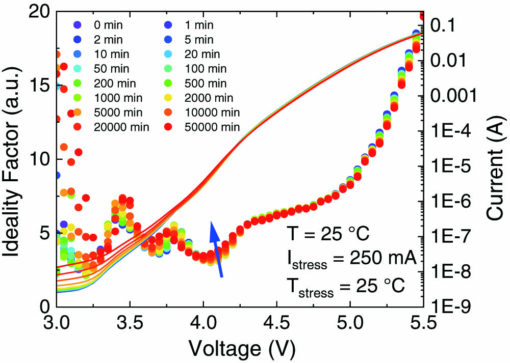
Figure
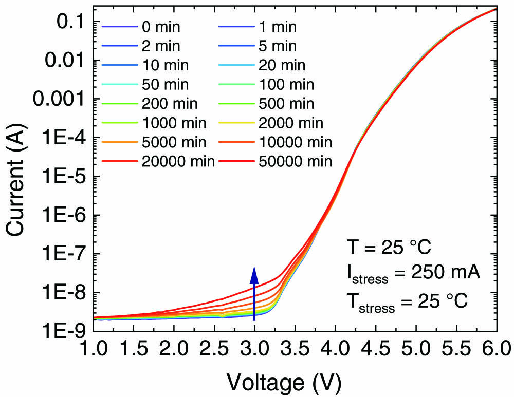
Fig. 1. Electrical characterization during the stress, in semi-logarithmic scale, carried out before and during the stress experiment at 250 mA. All measurements were taken at 25°C.
These results are confirmed also by the data reported in Fig.
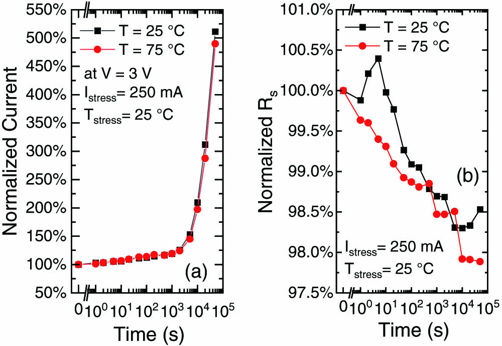
Fig. 2. (a) Normalized current at the voltage of 3 V, and (b) normalized series resistance (
We ascribed the increase in the sub-turn-on current at the generation of mid-gap states during the stress, confirmed also by the calculation of the ideality factor (Fig.
With regard to the optical degradation, Fig.
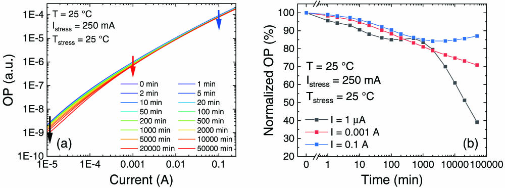
Fig. 4. (a) Optical power (OP) during the stress at the temperature of 25°C. (b) Normalized optical power at three different current levels: 10 μA, 1 mA, and 100 mA.
We start considering the behavior of the devices as observed for high current levels (100 mA), i.e., in the regime where the behavior of the devices is not significantly influenced by SRH recombination. We suggest that the optical degradation detected at high current levels is due to a worsening of the injection efficiency. This is consistent with the fact that up to 1000 min of stress the degradation rate is almost independent on the measuring current level [see Fig.
Several mechanisms can contribute to this variation in injection efficiency. A first process is the decrease in hole concentration at the p-side, due to a partial compensation of the acceptor dopant through the formation of Mg-H bonds [18,19]. This process is not supposed to play a major role, since it would result in a significant increase in the series resistance, which is not observed here [as shown in Fig.
A second mechanism that impacts on the injection efficiency is carrier escape [20]. However, escape is a thermionic process, following an equation like , where is the diffusion constant, is the diffusion length, is the effective density of states in the active region, is the height of the barrier, and is the Fermi level [20]. The rate of escape mainly depends on the height of the confinement barrier at the p-side of the quantum wells, which is not supposed to change as a consequence of stress.
A third mechanism that can lower the injection efficiency is the generation of charged defects in the active region [21]. Such charged defects may modify the band bending near the quantum wells (QWs), thus making carrier injection more difficult (Fig.
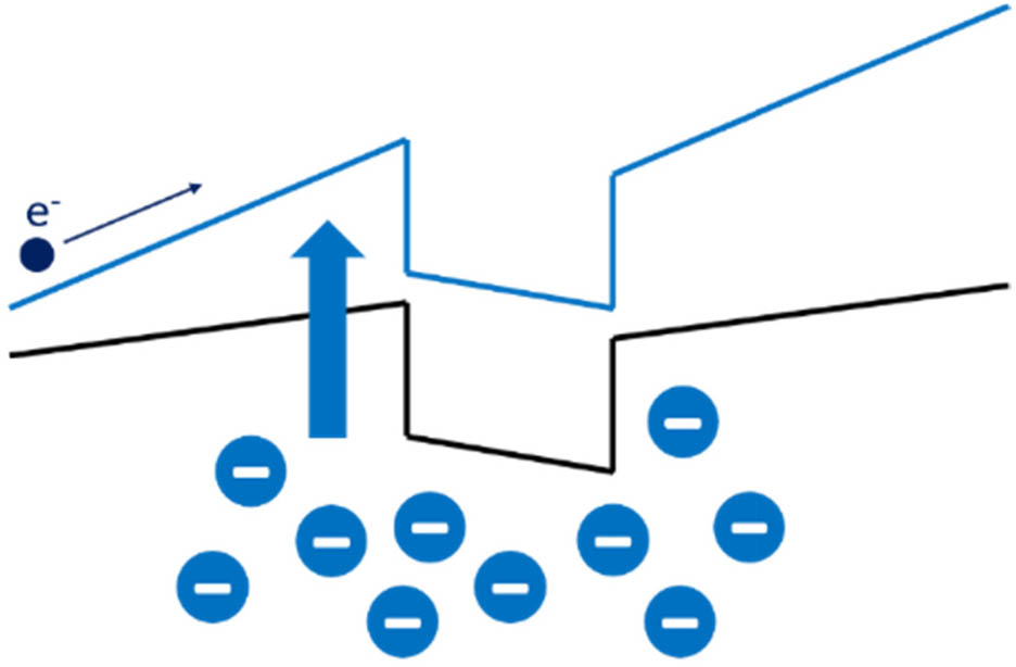
Fig. 5. Simplified representation of the increase in the injection barrier due to the presence of a distributed negative charge near/within the active region.
As a plausible model, we consider that stress induces the generation of negatively charged defects near/within the active region. A possible process can be the de-hydrogenation of (previously) hydrogenated gallium vacancies, which are naturally present in MOCVD-grown (metal organic chemical vapor deposition) gallium nitride.
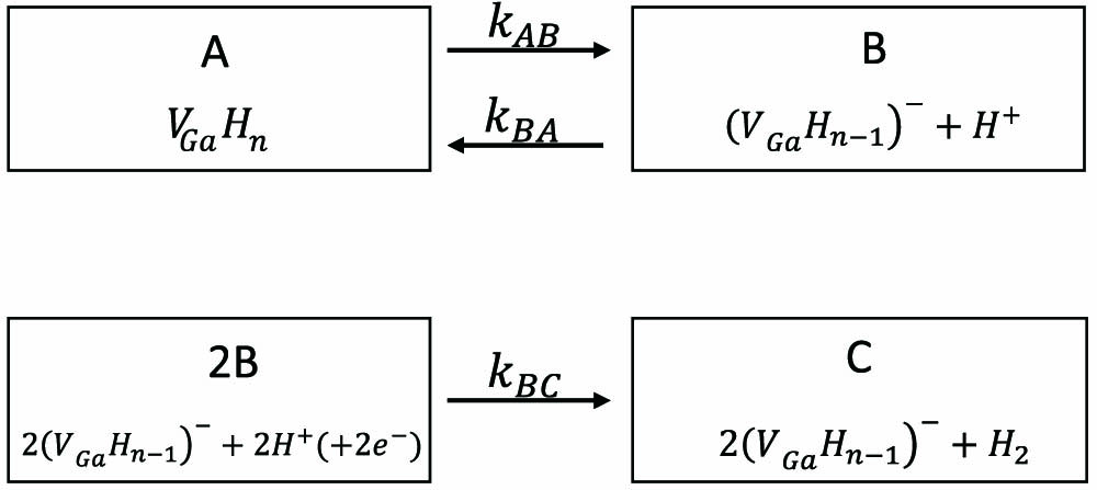
As discussed in Ref. [22], de-hydrogenation of Ga vacancies, leads to an increase of acceptor concentration. This reaction may be promoted by the flow of carriers through the active region of the devices, and/or by the energy released by non-radiative recombination events (for instance, Auger recombination [23]). Since ions have a high mobility, they may then re-bond with a gallium vacancy or find another hydrogen atom to form molecular hydrogen (with the contribution of two electrons). The processes could be described like in Fig.
The Ga vacancies (state ) could de-hydrogenate into (state , rate coefficient ). State is metastable: this means that the hydrogen ion is free, and could either re-bond with a de-hydrogenated vacancy (going back to state , with rate coefficient ), or find a second hydrogen atom to form molecular hydrogen (going to state , with rate coefficient ). In this second case, the hydrogen finds a stable form, and leaves behind a de-hydrogenated vacancy , that modifies the injection efficiency, as described above. These processes could be described by the following system of ordinary differential equations (ODEs): Here represents the number of hydrogenated vacancies, is the number of de-hydrogenated vacancies with neighboring -atom (, and is the number of de-hydrogenated vacancies without H-atom (acting as acceptors).
After defining this system of equations, we solved them numerically, after imposing as a boundary condition that the initial value of is equal to 1. The coefficients were obtained numerically, as fitting parameters. As shown in Fig.
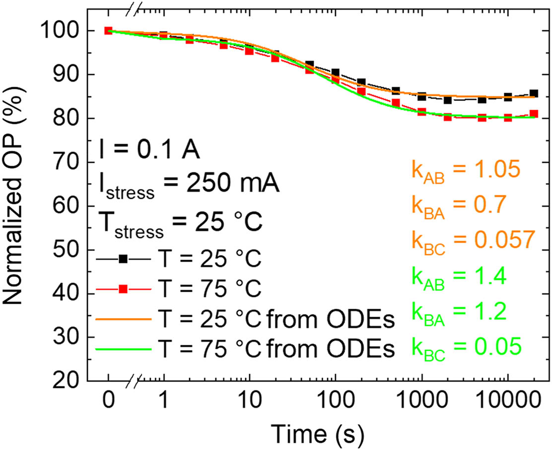
Fig. 7. Optical degradation measured at 25°C and 75°C during stress at 250 mA. Solid lines represent the solution of the system of ODEs reported above, showing a good agreement with the experimental data.
Thus, we conclude that the proposed model is able to predict the variation in optical power during stress time for high measuring current levels, i.e., in the regime where the variation in injection efficiency is the dominant degradation process.
For low current levels, a different trend is observed. Specifically, after the first phase () has ended, a second mechanism is observed, for . This second process has a stronger effect at low measuring current levels, and it is ascribed to an increase in the non-radiative recombination rate, due to the generation of defects.
We can explain the behavior at low current density, with the hypothesis formulated by Ruschel et al. [24], where the authors indicated that the optical power has the following behavior for long operation time: where is the current density, is the stress time, and and are two fitting parameters. This is in agreement with the results in Fig.
![Fitting of the optical power data at low current level with the function proposed in Ref. [24].](/richHtml/prj/2020/8/11/11001786/img_008.jpg)
Fig. 8. Fitting of the optical power data at low current level with the function proposed in Ref. [24].
A possible scenario for long stress time considers the generation of non-radiative recombination centers due to the energy released by Auger recombination events. The consequent increase in SRH recombination coefficient has an impact, which is stronger for low measuring current levels, as predicted by the well known ABC rate equations. The contribution of this mechanism is negligible in the first phase of the stress, compared to the effect given by the drop in injection efficiency described above.
So, the long-term degradation measured at low current levels can be ascribed to the generation of non-radiative centers, possibly caused by the energy released by Auger recombination events.
In Fig.
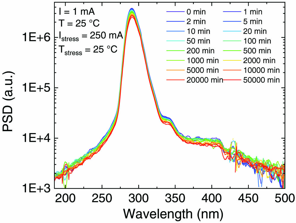
Fig. 9. Power spectral density during the aging at the current of 1 mA and at the temperature of 25°C.
According to the SRH theory, the defects that have a stronger effect on the optical characteristics of LEDs are those located near the mid-gap [20]. Similarly, recent papers indicated that the defects that have the stronger impact on the sub-turn-on leakage components are located close to the mid-gap [15,16]. For this reason, we carried out an extensive analysis to identify the generation of traps near the active layer of the devices, by capacitance spectroscopy. To this aim, normal deep-level transient spectroscopy cannot be used, since the time constant of the capacitance transients would be too long for practical implementation of the technique.
In fact, the time constant for emission can be calculated as With , and , time constants in excess of would be obtained even at high temperature (500 K), for mid-gap defects.
For this reason, we decided to opt for SSPC measurements. This method uses monochromatic light excitation to favor a fast ionization of defects, thus particularly effective for the study of very deep defects in wide bandgap semiconductors.
In Fig.
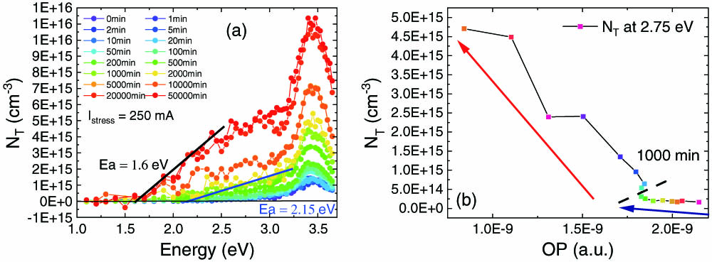
Fig. 10. (a) SSPC measurement during the aging, and (b) correlation between the second defect from SSPC and the optical power at low current levels.
3. CONCLUSIONS
In this work, we presented an extensive analysis of the behavior of UV-C LEDs during the constant current stress test. We found the presence of two different degradation mechanisms.
The first one is dominant in the first 1000 min of stress, and it is ascribed to a decrease in the injection efficiency. It causes a decrease in the optical power and in the amplitude of the main peak of the emission spectra, which is independent of the measuring current level. The related kinetics were modeled by considering the defect-reaction dynamics responsible for the de-hydrogenation of gallium vacancies, through a system of three differential equations. The results show a good agreement with the experimental data, supporting the validity of the model.
The second mechanism is dominant after 1000 min of stress, and it is correlated to the generation of mid-gap defects. It leads to an increase in the sub-turn-on current, and a decrease in the optical power and in the PSD main peak, especially at low current levels. Moreover, we found evidence of this defect generation from the slope of the optical power characteristics at low current levels, from the ideality factor, and from the results of SSPC measurement, which indicates the generation of defects at .
In a future work, microscopy techniques (transmission electron microscopy, scanning electron microscopy, energy dispersive X-ray analysis, positron annihilation spectroscopy) could be used to experimentally evaluate the impact of electrical stress on the microscopic properties of the material. Also, positron annihilation spectroscopy could be used to evaluate the role of vacancies in the degradation process.
4 Acknowledgment
Acknowledgment. This research was partly performed within the project INTERNET OF THINGS: SVILUPPI METODOLOGICI, TECNOLOGICI E APPLICATIVI, co-founded (2018-2022) by the Italian Ministry of Education, Universities and Research (MIUR) under the aegis of the “Fondo per il finanziamento dei dipartimenti universitari di eccellenza” initiative (Law 232/2016).
F. Piva, C. De Santi, M. Deki, M. Kushimoto, H. Amano, H. Tomozawa, N. Shibata, G. Meneghesso, E. Zanoni, M. Meneghini. Modeling the degradation mechanisms of AlGaN-based UV-C LEDs: from injection efficiency to mid-gap state generation[J]. Photonics Research, 2020, 8(11): 11001786.
