1. INTRODUCTION
Surface plasmon polaritons (SPPs) are electromagnetic waves propagating along metal–dielectric interfaces with exponential decay in the direction vertical to the interface. SPPs with the nature of subwavelength confinement and strong field enhancements have found promising applications in superresolution imaging [1], high-density optical data storage [2], and sensitivity biosensors [3–6" target="_self" style="display: inline;">–6]. Among these, SPP-based plasmonic circuits have attracted much attention because they possess the capacity to both carry photonic information and miniaturize electronics, which opens up a new way for the next generation of integrated circuits, especially in information processing and transmission [79" target="_self" style="display: inline;">–9]. In an effort to realize subwavelength waveguides and compact integrated circuits, it is vital to excite and control SPPs. This is undoubtedly of great interest not only for the optical frequency but also for the lower frequencies. However, from the optical to the far-infrared and terahertz (THz) range, the frequency-dependent metal dielectric constant undergoes drastic change. At THz frequencies, since most metals behave as perfect electrical conductors, the surface does not support bound modes of THz surface waves [10]. Therefore, for a long time, SPPs have been considered to exist only at optical frequencies.
In order to realize high-confinement SPPs at microwave and THz frequencies, corrugated metallic structures are proposed to support and propagate the SPPs, called spoof SPPs [1113" target="_self" style="display: inline;">–13], which display very similar features in dispersion properties, subwavelength confinement, field enhancements, and environment sensitivity as those of the optical SPPs [1416" target="_self" style="display: inline;">–16]. Much effort has been put into generating highly confined spoof SPPs with desired functions at microwave and THz frequencies [17–22" target="_self" style="display: inline;">–22]. Cui et al. have demonstrated the guiding of spoof SPPs on ultrathin metal films to a very long distance at microwave frequencies [20]. Meanwhile, some spoof SPP functional devices, such as amplifications, wavelength filters, and sharp bends, have also been reported [22–26" target="_self" style="display: inline;">–26]. In the THz regime, guiding highly confined SPPs along corrugated metal structures, such as periodic grooves or pillars, have been proposed [1719" target="_self" style="display: inline;">–19,27]. However, due to the lack of an efficient and expedient THz near-field measurement method, most of the previous works are limited to the numerical simulations or indirect far-field detections [18,2830" target="_self" style="display: inline;">–30]. Directly quantifying the performance of THz spoof SPPs and effectively manipulating them still remain as challenges. Inspired by this, in this paper, we theoretically and experimentally demonstrate a THz spoof SPP waveguide structure consisting of periodic metallic rectangular pillars. Based on our recently developed scanning near-field THz microscopy (SNTM), the electric field distributions around the metal surface can be detected by a small near-field probe. The properties of the waveguide, including propagation length, horizontal confinement, and spatial evanescent extension, can thus be estimated. Based on the measured properties, a series of waveguide components, including an S-bend, a Y-splitter, and some directional couplers (DCs), were designed and studied experimentally. We identify directly and quantitatively the propagation, bending, splitting, and coupling of spoof SPPs from the mapping electric field distributions. Our presented results definitely show that such a structure can be designed arbitrarily to achieve fruitful controlling of spoof SPPs at THz frequencies. This kind of plasmonic structure with good functionality would lead to the development of more robust and complex THz functional devices.
2. DISPERSION AND ANALYSIS OF THE SPOOF SPP MODE
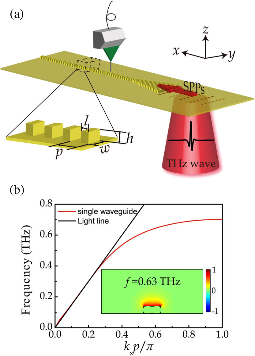
Figure 1(a) shows the schematic of the chosen waveguide structure with a row of periodic metal pillars arrayed on the metal surface. Previous studies have demonstrated that the geometrical sizes of the metal structure have a significant influence on the dispersion relation of the SPP mode [17,18,31,32]. Hence, we chose the parameters as , , , and . Figure 1(b) shows the dispersion relation ( versus frequency) of the waveguide structure calculated using the eigenmode solver of the commercial software CST Microwave Studio. In the numerical modeling, one unit cell of the waveguide structure was considered. The bottom of the waveguide and pillars were assumed as the perfect electrical conductors. A periodic boundary condition was used in the direction, and the phase variation in direction was . Based on the equation , the values of were obtained. Within the first Brillouin zone, the of the SPP mode became larger than the light line (black line) with increasing frequency, which means that the textured surface with pillars possesses good field confinement ability. The inset of Fig. 1(b) displays a lateral profile of the normalized electric field component () of the SPP mode at 0.63 THz. It is apparent that the electric field was confined tightly around the surface of the pillar. From Fig. 1(b), we can see above 0.5 THz that SPP modes can be supported and propagate along the surface of the metal structure. However, at around 0.7 THz, the group velocity of the SPP mode decreased to zero gradually at the first Brillouin zone boundary ().
Fig. 1. (a) Illustration of the experimental setup. The inset shows a schematic of the waveguide structure with the following geometrical parameters: the period , the width , the length , and the depth of the pillar. (b) Dispersion relation of the SPP mode for one row (red line) of metal pillars. The inset is the normalized field magnitude of the electric field component () for the cross section of a single-row waveguide at 0.63 THz. The dashed line indicates the boundary between metal and air.
下载图片 查看所有图片
3. EXPERIMENTAL RESULTS AND ANALYSIS
Different waveguide components to be investigated include a straight waveguide, an S-bend, a Y-splitter, and DCs. To fabricate high-quality waveguide components, traditional fabrication technologies were adopted. The pillars were formed by optical lithography on a silicon substrate, followed by deep reactive ion etching. A 200 nm thick gold film was then coated on the chip, including the sidewalls of the pillars in a gold sputter coater. The waveguide components were studied experimentally using a fiber-coupled SNTM operating at 1.56 μm. Figure 1(a) illustrates the experimental measurement process, where the THz waves impinge on the excitation area of the sample and then the excited SPPs are detected by a near-field probe with a resolution of 8 μm. Coupling of free-space THz radiation to excite the SPPs was achieved by periodic hole arrays, where rectangular holes with dimensions of were arrayed on the thin metal with a period of 485 μm along the direction and 250 μm along the direction. The total excitation area was . The condition to excite SPPs should ensure that the direction of the linearly polarized THz wave was perpendicular to the hole gratings as well as parallel to the propagation axis of the waveguide. Furthermore, a funnel structure consisting of pillars was designed to efficiently couple the SPPs to the waveguide [33]. In this design, the period of the pillars in the funnel structure was the same as the waveguide structure. The initial funnel width was 1.5 mm, and the length was 1.6 mm. The methods of excitation and funnel structure were applied in all waveguide components. The performance of the waveguides was characterized by mapping the near-field distribution above the waveguide surface. The THz probe was placed above the sample with a distance of 130 μm and scanned the signals point by point with a step of 100 μm along the direction and a step of 200 μm along the direction.
3.2 A. Straight Waveguide
Straight waveguides are fundamental elements for integrated optical circuits, and, as a result, it is important to understand their propagation characteristics. Based on the periodic structure introduced previously, a straight waveguide with a length of 5 mm was fabricated and characterized. Figure 2(a) shows a scanning electron microscopy (SEM) image of a part of the straight waveguide. The scanning area was , and the excitation area and funnel structure were not taken into account. The normalized power () of the straight waveguide was imaged at 0.58 THz [Fig. 2(b)]. The near-field image demonstrates well-confined SPPs guiding along the waveguide structure. Based on the field amplitudes measured, the propagation length, horizontal confinement, and field attenuation along the direction were quantitatively estimated. Figure 2(c) plots the measured amplitudes (blue dots) as a function of distance with an exponential fit (red line), which reveals a propagation length of 9.2 mm. The corresponding propagation loss was about 8 dB/cm. Figure 2(d) displays the normalized field amplitude as a function of the coordinate at , which shows a full width at half-maximum (FWHM) of approximately 400 μm. The degree of field attenuation along the direction also demonstrates the ability to confine SPPs for the waveguide. Thus, the amplitude, which was measured at the waveguide center, was sampled as a function of distance from the surface [red dots in Fig. 2(e)]. The spatial evanescent extension (distance where the field drops to of the surface value) in the air was 197 μm obtained by an exponential fit [solid line in Fig. 2(e)]. Compared to a bare metal surface, the spatial extension of the textured surface with pillars was reduced by several orders of magnitude.
Fig. 2. (a) SEM image of the straight waveguide. (b) Near-field image of the straight waveguide. The normalized power distribution at 0.58 THz is shown. (c) Amplitude attenuation as a function of propagation distance. Blue dots represent experimental results, and the solid line is the exponential fit. (d) Measured electric field amplitude along the line , showing the horizontal confinement. (e) Amplitude as a function of increasing . The red dots are experimental results, and the solid line is the exponential fit.
下载图片 查看所有图片
3.3 B. S-Bend Waveguide and Y-Splitters
On the basis of the above study of the straight waveguide, one could envisage that the tightly bound SPPs by the textured surface could be guided along a nonstraight path. An S-bend waveguide based on the cosine function was designed [34]. The S-bend waveguide component was used as a junction to connect two straight waveguides offset with respect to each other. An S-bend waveguide component was also a basic element for a Y-splitter, which was composed of two mirrored S-bends. Figure 3(a) shows a schematic of the S-bend and Y-splitter waveguides. There is a lower loss with an increasing radius of curvature for a bend [35]. With low loss taken into consideration, the S-bend with a radius of curvature of 911.8 μm was fabricated and also applied in the Y-splitter. The S-series waveguides were studied in a similar way by recording the electric field above the surface. For the S-bend waveguide, the normalized power at a frequency of 0.58 THz is exhibited in Fig. 3(b), with a scanning area of . The result demonstrates well-confined SPPs guiding throughout the structure. The power attenuation was estimated to be 15 dB/cm through the bend. Figure 3(c) delineates the normalized power distribution of the Y-splitter waveguide at 0.58 THz. At the junction, the two beams were separated successfully. At the end of the waveguide, the two arms were separated within a distance of 3 mm. For a quantitative evaluation of the input and output powers, the normalized data along the lines and are shown in Fig. 3(d). The power in each branch was almost same. At the end of the waveguide, the low power might be caused by the ending echo.
Fig. 3. (a) Schematic of S-bend and Y-splitter waveguides. Near-field images corresponding to (b) S-bend and (c) Y-splitter waveguides. The normalized power distribution at 0.58 THz is shown. (d) Measured amplitude of the electric field as a function of the coordinate along the lines (input) and (output) of the Y-splitter.
下载图片 查看所有图片
3.4 C. DC
In addition to the waveguide components described above, there is still more potential to realize different functional plasmonic components based on the proposed structure, such as DCs. DCs can be used as wavelength-selective components for filtering and separation of wavelengths, which are essential in the realization of demultiplexing components [36,37]. The structure of a DC is displayed in Fig. 4(a). There are two sections consisting of straight waveguides and S-bend waveguides. The first part comprises two parallel straight waveguides, the gap between them is , and the length of the parallel section is , which is treated as the interaction region. Following the straight waveguides, S-bend waveguides were connected to separate the waves. To investigate the effect of change of on the coupling of the two waveguides, the supermode approach was applied for analysis. When two identical waveguides are close to one another, there are two modes supported by the entire structure. In Fig. 4(b), the normalized electric distributions () of the two modes for the cross section at 0.63 THz are displayed. The upper one is the even mode, and the lower one is the odd mode. To obtain the dispersive relations of the two eigenmodes, the same numerical simulation introduced before was adopted. As we can see in Fig. 4(c), the propagation constants of the even modes () and the odd modes () as functions of frequency for different values of varied from 115 to 50 μm were plotted. For the even mode, there is little influence of different values of on the dispersion relation. However, for the odd mode, becomes larger with increasing at the same frequency. Thus, the difference between the two modes is larger for DCs with a smaller gap . The difference between these two modes at the same frequency will lead to a phase difference . After the SPPs have propagated a distance, the accumulated phase difference reaches a value of , and the mode power will be shifted completely from one waveguide to the other. The length corresponding to this shift is defined as the coupling length, which can be expressed as . For two parallel waveguides with different values of of 115, 90, 70, and 50 μm, the coupling length as a function of frequency from 0.5 to 0.65 THz can be obtained [Fig. 4(d)]. It is observed that the coupling length has a weak dependence on frequency from 0.55 to 0.65 THz. However, the increase of causes a lager coupling length at 0.6 THz, as shown in Fig. 4(d) (blue area). The coupling length decreases from 2.83 to 1.46 mm when is changed from 115 to 50 μm.
Fig. 4. (a) Schematic of the DC with relevant parameters. (b) Normalized electric component () distribution for the cross section of even (upper) and odd modes (lower) supported by two parallel waveguides. (c) Dispersion relation of even and odd modes for DCs with varying . (d) Calculated coupling length for DCs with different values of 115, 90, 70, and 50 μm.
下载图片 查看所有图片
In order to verify the numerical analysis, several DCs with different values of 50, 70, 90, and 115 μm were fabricated. One of the straight waveguides was connected to the SPP source [the input in Fig. 4(a)]. The length of the coupling section was kept at in all DCs. The near-field images obtained with normalized power at 0.6 THz are shown in Figs. 5(a)–5(d). In these pictures, the gap between the parallel waveguides is 115, 90, 70, and 50 μm, respectively. For the DC with , the length of the interaction region is identical with the coupling length, so the SPPs were coupled to another waveguide all completely and transmitted from output 2. The experimental results presented in Fig. 5(a) show a good consistency with numerical calculation. For the DCs with and 70 μm, the coupling length is smaller than the length of the interaction region. In these cases, the coupling between the two parallel waveguides was still continuing throughout propagation of the coupling length. Thus, some parts of the SPPs were coupled back into the first waveguide and transmitted from output 1 and the left part transmitted from output 2 [Figs. 5(b) and 5(c)]. For the DC with , the coupling length becomes about half of . The numerical calculations indicate that most of the SPPs should couple back to the first waveguide. However, we notice that some of the SPPs still existed in the second waveguide. This might be caused by the coupling between the two waveguides in the S-bends [36]. In Figs. 5(e)–5(h), the field amplitudes of the cross sections at the input (line ) and end of the straight waveguides (line ) are displayed as a function of decreasing . In these pictures, the amplitudes of the input at were almost the same. For the amplitudes recorded at the end of the straight waveguides, the field at was gradually increased with decreasing , and the amplitude at had the opposite trend. This component thus has a potential to function as a beam splitter with an active control of the splitting ratio.
Fig. 5. (a)–(d) Normalized power distributions for DCs at 0.6 THz. (e)–(h) Field amplitudes of cross sections at the input (line ) and end of straight waveguides (line ) corresponding to DCs with , 90, 70, and 50 μm from left to right, respectively. Lines and are represented as dotted lines in (a)–(d).
下载图片 查看所有图片
4. CONCLUSION
In summary, one kind of plasmonic structure of strong ability in manipulating THz spoof SPPs was theoretically and experimentally studied. We identified the performance of spoof SPPs quantitatively based on the SNTM measurements. Tightly confined SPPs with a spatial evanescent extension of 197 μm were proved to propagate along the subwavelength waveguide. An FWHM of 400 μm and a propagation length of 9.29 mm were achieved. Based on the proposed structure, different waveguide components, including a straight waveguide, an S-bend, a Y splitter, and DCs, were designed and characterized. We demonstrated that these waveguide components could realize power splitting, wave bending, wave coupling, and wavelength selection. It is believed that the proposed waveguide offers promising approaches for developing new THz guided-wave devices and is thus useful in compact THz integrated plasmonic circuits.
Ying Zhang, Yuehong Xu, Chunxiu Tian, Quan Xu, Xueqian Zhang, Yanfeng Li, Xixiang Zhang, Jiaguang Han, Weili Zhang. Terahertz spoof surface-plasmon-polariton subwavelength waveguide[J]. Photonics Research, 2018, 6(1): 01000018.
 Download: 1171次


