Photonics Research, 2018, 6 (6): 06000653, Published Online: Jul. 2, 2018
Spatially resolved measurement of plasmon dispersion using Fourier-plane spectral imaging
Figures & Tables
Fig. 1. Schematic sketch of the measurement system (a) in real-space imaging mode and (b) in Fourier-plane imaging mode. The dashed red lines illustrate the evolution of a single plane wave entering the prism and propagating through the setup in Fourier-plane imaging mode. (c) A subsection of a resolution target, as imaged through the optical system in the real-space imaging mode. (d) Real-space intensity distribution at the sample plane after focusing by L1. (e) Intensity distribution in Fourier-plane imaging mode for an incoming collimated beam. The dashed vertical lines in (d) and (e) mark the edges of the spectrometer entrance slit.
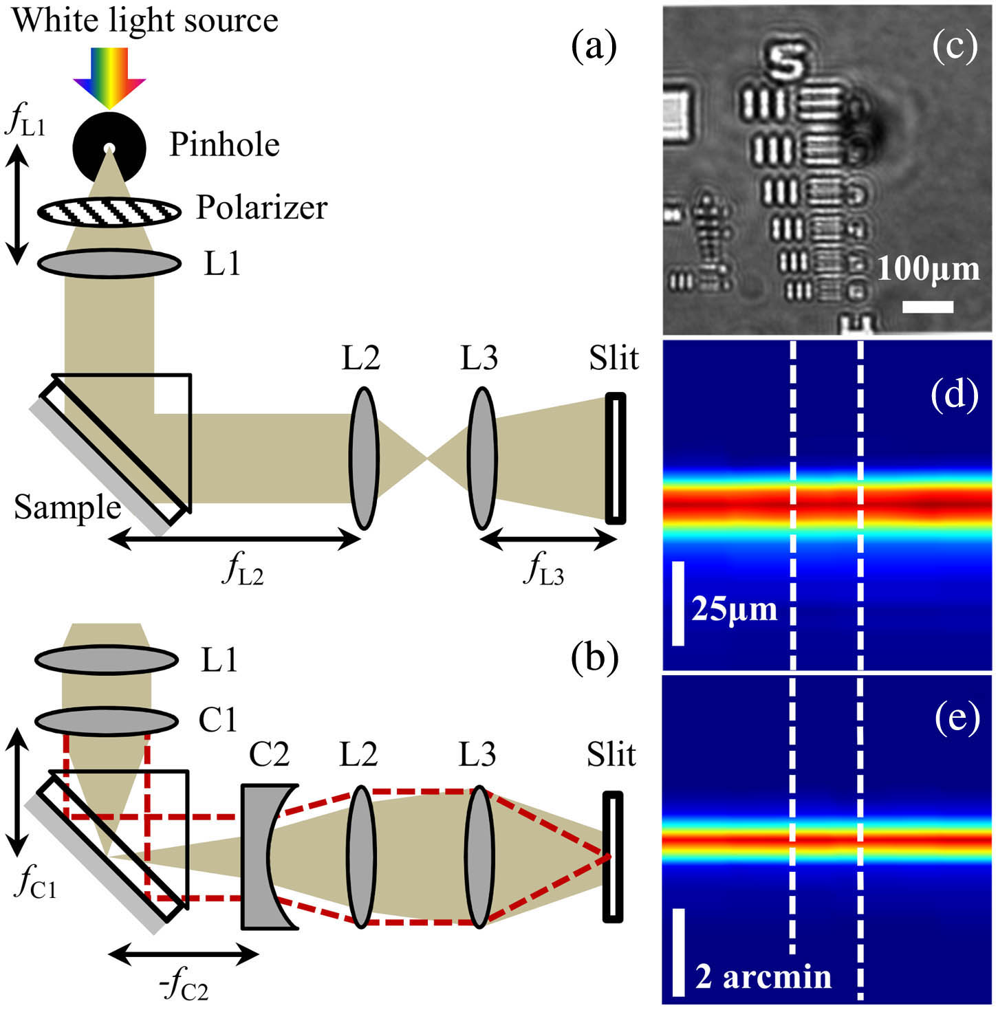
Fig. 2. Reflected intensity maps recorded for an Ag film for (a) TE and (b) TM polarizations. (c) Dispersion diagram of the SPP on an Ag film, measured by Fourier-plane spectral imaging. The solid line shows the SPP dispersion curve calculated by the T-matrix method. (d) Measured dispersion curve for an Ag film covered with a PVA/TDBC layer, exhibiting normal-mode splitting as a result of strong coupling between SPPs and molecular excitons. The solid lines show the dispersion curve calculated by the T-matrix method with the PVA thickness and the molecular absorption as free parameters.

Fig. 3. (a) Optical microscope image of the fabricated metal-strip waveguides. The numbers indicate the widths of the individual waveguides. (b) A schematic sketch of a waveguide cross section.

Fig. 4. SPP dispersion measured by Fourier-plane spectral imaging (a) for a 200 μm × 200 μm Al 2 O 3 w = 50 μm w = 10 μm w = 3 μm Al 2 O 3

Amir Ohad, Katherine Akulov, Eran Granot, Uri Rossman, Fernando Patolsky, Tal Schwartz. Spatially resolved measurement of plasmon dispersion using Fourier-plane spectral imaging[J]. Photonics Research, 2018, 6(6): 06000653.


 PDF全文
PDF全文

