On-chip reconfigurable mode converter based on cross-connected subwavelength Y-junctions  Download: 626次
1. INTRODUCTION
On-chip optical interconnect has enticed wide attention due to its several appealing features, such as high bandwidth, low power consumption, and compact footprint [1,2]. To cope with the ever-increasing information capacity, wavelength-division multiplexing and polarization-division multiplexing have been intensively explored and successfully deployed in optical interconnect on-chip integration [3,4]. Ever-exploding networking traffic, however, demands for more cost-effective optical interconnects. Recently, mode-division multiplexing (MDM) has provided a new dimension to further enlarge communication capacity by using different spatial modes of waveguides to individually carry optical signals [5–7]. Mode converters are fundamental components for multiplexing and switching among such information channels. In addition, it is of great interest to develop reconfigurable optical interconnects so that bandwidth and channels can be utilized optimally and flexibly [8,9]. Several mode converters have been previously proposed. The directional coupler-based scheme [10,11] can achieve high-performance mode conversions by precisely designing waveguide width, coupling gap, and coupling length; such couplers can also be conveniently used for mode multiplexing and demultiplexing. In addition, the mode conversion can be realized using the adiabatic evolution-based scheme [12,13], such as asymmetric Y-junctions or adiabatic tapers. Another interesting scheme is to rely on inversely designed subwavelength structures [14,15] to achieve mode conversion in a more compact footprint. In the above-mentioned three types of devices, however, the mode conversion is reconfigured at the cost of large modulation of material refractive index [16,17], which hinders their practical applications. Recently, cascaded three-waveguide-coupling structures are successfully utilized to realize a reconfigurable mode converter [18]. On the other hand, Mach–Zehnder interferometer-like (MZI-like) structure [19,20] is a promising scheme for implementation of a reconfigurable mode converter. The principle is stated as follows: the th-order mode () can be effectively considered as a mode array, which is a combination of fundamental modes with fixed amplitude and phase distribution. Mode conversion is realized when a structure allows the modes of the array to individually travel through different phase shifters thus ending in another phase distribution. An MZI-like structure usually is composed of parallel-connected symmetric Y-junctions or multi-mode interferometers (MMIs). For the MMI, it is difficult to support more than two modes due to its poor self-imaging performance for higher-order modes [21,22]. In Ref. [20], a four-mode reconfigurable converter based on multi-layer parallel-connected symmetric Y-junctions is proposed, while its fabrication relies on either direct laser writing or a non-standard/multi-step lithography process [23,24]; the inconvenient fabrication methods hinder cost-effective and large-scale integration deployment. Meanwhile, such a parallel-connected structure required that the number of electrodes applied to drive the phase shifters is proportional to the number of modes that can be reconfigured, which means the power consumption is proportional to the number of operating modes.
In this work, we propose a novel single-step-etched reconfigurable mode converter based on cross-connected symmetric Y-junctions on a planar silicon platform. For ease of fabrication and reliable operation, subwavelength symmetric Y-junctions are chosen in our design. Thin-film electrode heaters are employed to control the phase difference between the mode array propagating through the Y-junctions. With this structure, any mode launched into a waveguide at one end can be converted into any other mode at the other end. The number of modes that can be reconfigured depends on the mode splitting ability of the Y-junction. The converter exhibits ultra-low power consumption, since the number of electrodes can be reduced by half compared to the parallel-connected one. We have designed and fabricated the converter to achieve switchable conversions between any two of the first four TE modes. The measured average insertion losses (ILs) for all different conversions are 1.71–2.45 dB while the average cross talks (XTs) are less than over an operating bandwidth of 60 nm centered at 1.56 μm, respectively. The minimum and maximum power consumptions applied to the conversions are less than 10 mW and 75 mW, respectively. Such a power-efficient, CMOS-compatible, and scalable mode converter may become an important building block in future high-capacity and large-scale on-chip optical networks.
2. DEVICE DESIGN AND OPERATION PRINCIPLE
The schematic configuration of the on-chip reconfigurable mode converter for four modes is shown in Fig. 1(a). The device is designed on a silicon-on-insulator (SOI) wafer with a 220-nm-thick top silicon layer over a 2-μm-thick buried oxide layer, and covered by a 1.2-μm-thick capping layer. Without loss of generality, we consider only TE modes in this study. The input and output waveguides support the , , , and modes. In our design, two four-mode symmetric Y-junctions () and four dual-mode symmetric Y-junctions () are used. At the input end, the four-mode waveguide is split into two halves by and each half is further split into two halves by , which can be considered as a Y-junction. The four branches support only the fundamental mode. Key geometrical parameters that define the Y-junctions are as labeled in Fig. 1(b). A single-mode waveguide crossing based on a 90°-crossed MMI [25], is introduced to connect the middle two branches. As shown in Fig. 1(c), the waveguides connecting the branch and the MMI waveguide are linearly tapered from to within a length of , and the length of the MMI waveguide is . In order to balance the initial phase difference, the four branches are designed to have the same effective lengths. Similarly, at the output end, the four branches are recombined into a four-mode waveguide with another pair of and a . By taking advantage of the cross-connected structure, only two electrode heaters, and , are deposited on the upper dual-mode branches of , respectively, to provide thermo-optic control of the refractive indices of the branches and hence the phase difference between the mode array propagating through the Y-junctions. In this way, the phase shifters can work for the or mode.
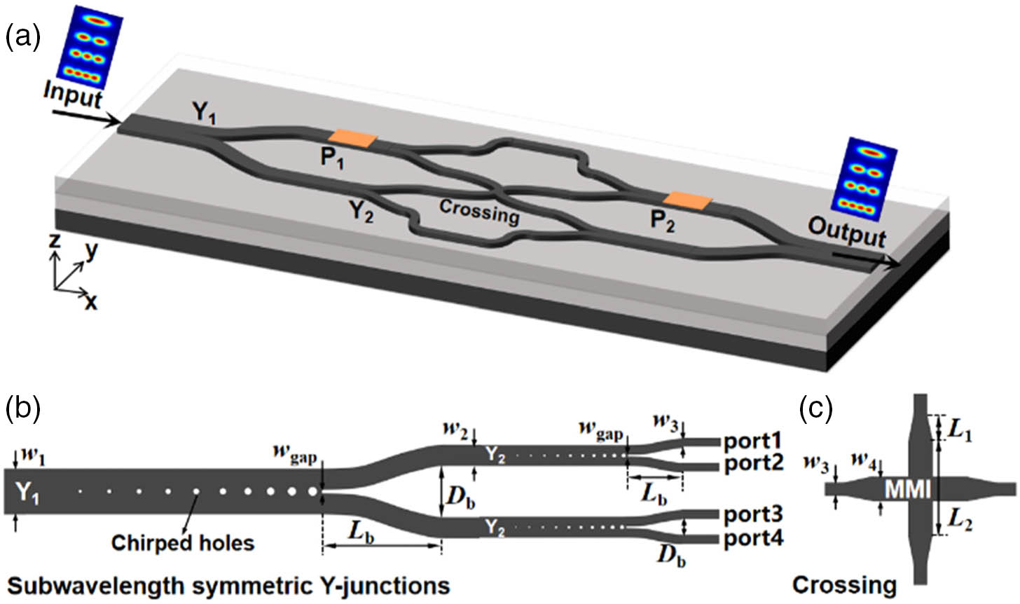
Fig. 1. Schematic diagrams showing (a) the structure of the proposed mode converter consisting of cross-connected symmetric Y-junctions, (b) subwavelength four- and dual-mode symmetric Y-junctions, and (c) single-mode waveguide crossing.
Here, the multi-mode symmetric Y-junctions can convert the ()th- or ()th-order mode () in the stem to two in-phase or anti-phase th-order modes in two branches. Notice in Fig. 1(b) that Y-junctions based on subwavelength holes are used. If a conventional adiabatic Y-junction is used, a slightly blunt gap owing to inherent lithography limitation will deteriorate their adiabatic property and result in large ILs and XTs, especially for even-order modes. Therefore, the subwavelength multi-mode symmetric Y-junctions with low ELs and XTs [26] are utilized. Our design uses a minimum feature size of 40 nm and the details of design can be found in Ref. [26]. The input stem of the () supports all , , , and modes, and the branches () support both the and modes. Then, the input stem of the supports both the and modes, and the branches () support only the mode. The gap widths at the branch interface of both and are . To keep the device compact, we set the branch lengths of and as 15 μm and 5 μm, respectively. The spacings between the two branches of and are 2.5 μm and 1.5 μm, respectively. The output power of the Y-junction, shown in Fig. 1(b), is important to the whole structure because it determines the input light state of the later reconfigurable operation. The corresponding transmission spectra are calculated via a 3D finite-difference time-domain method and shown in Fig. 2. The subwavelength Y-junction has uniform spectra, and the normalized power ratio of four output ports for all the four input modes is approximately 0.25:0.25:0.25:0.25 with a fluctuation of less than 0.0146 in the C band, which can ensure a fine bandwidth characteristic for our structure. For comparison, we also designed and simulated a conventional Y-junction in which conventional Y-junctions with a 40-nm branch gap were used instead. The curves presented in Fig. 2 clearly show that the output power of the conventional Y-junction is sensitive to wavelength and highly mode-dependent.
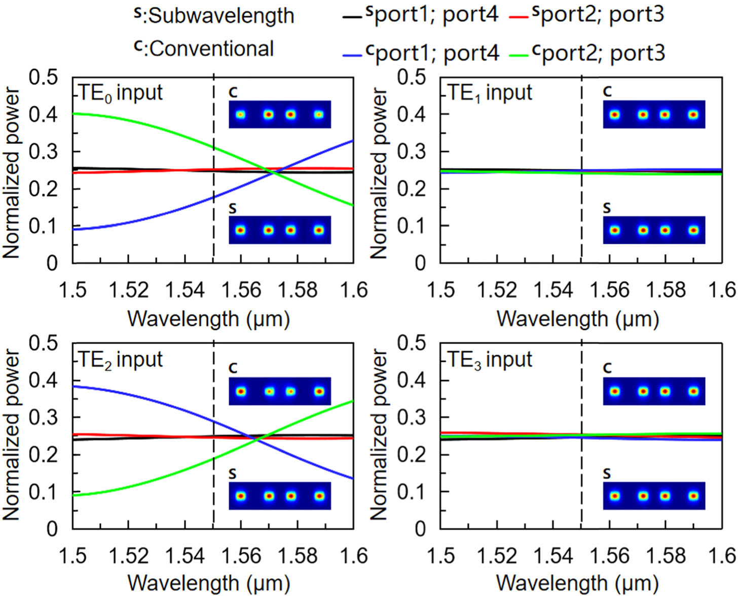
Fig. 2. Simulated normalized transmission spectra of the
When a waveguide mode is launched into the device, its field is split into four equal parts with fixed phase distributions, which propagate individually as the modes in the respective branches, as shown in Fig. 3. For instance, the mode has four equal parts with the same amplitude distribution and fixed relative phase distribution . They are combined at the output end by another set of Y-junctions and the combined mode depends on the phase differences between them, which is controlled by the voltages applied to the electrode heaters, and . The phase distribution (0 or ) among the middle two branches can be exchanged by the waveguide crossing. To facilitate discussion, we denote and as the optical phases in the corresponding branches generated by the heaters and . Assuming only the mode as the input mode, the operation principle is as follows. With ( and off), the output mode is the same as the input mode. When ( on) and ( off), an input will first split into four equal parts with a phase distribution (0, 0, 0, 0), which is converted to before waveguide crossing and after crossing; thus, a mode will emerge at the output end after recombination. Similarly, phase combination ( off) and ( on) will ensure that, for the input mode, the phase distribution changes from (0, 0, 0, 0) before crossing to at output, allowing conversion to a mode. When ( and on), for the input mode, the phase distribution changes from before crossing to at the output, resulting in a mode after recombination. It should be noted that, the output mode may be different from the input mode even if there are no phase differences introduced to the branches, for instance, the mode is converted to the mode and vice versa due to the intrinsic phase exchange along the cross-connected branches. On the contrary, the output mode will remain the same for the and modes when -phase differences are simultaneously introduced to both branches. The conversion functions of the device are summarized in Table 1. The same device could be employed to convert between two arbitrary compositions of the four modes by properly controlling the optical phases in the branches.
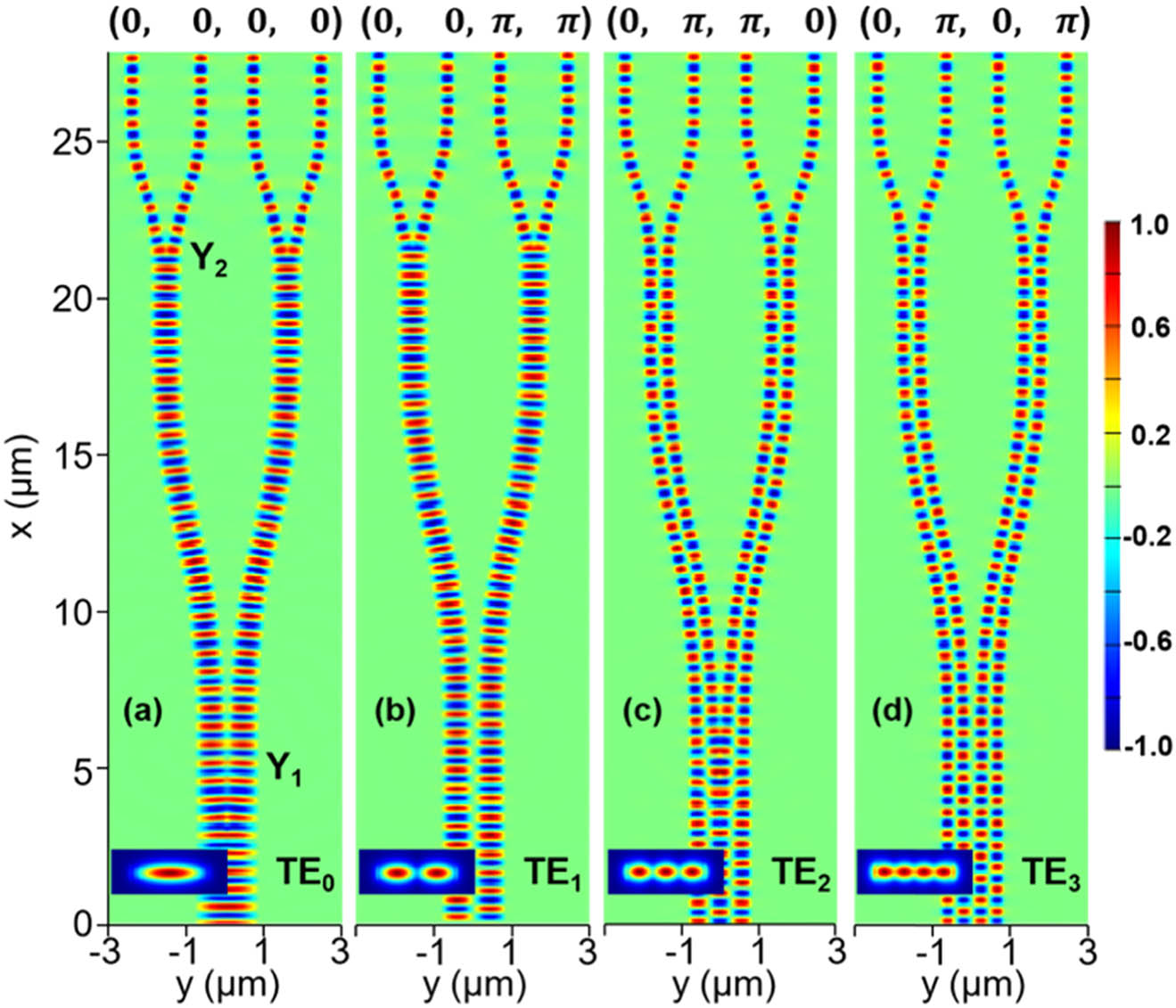
Fig. 3. Simulated distributions of the
We calculate the transmission spectra of the cross-connected converter via a commercial software (Lumerical INTERCONNECT). Assuming that no voltages are applied to the electrode heaters, the IL and XT profiles of the device are depicted in Figs. 4(a)–4(d) for the four input modes. The average ILs over the wavelength span from 1.5 μm to 1.6 μm for TE0, TE1, TE2, and TE3 inputs are about 0.45 dB, 0.40 dB, 0.50 dB, and 0.46 dB, respectively. Meanwhile, the average XTs for the four modes are –28.4 dB, –29.0 dB, –30.0 dB, and –29.2 dB, respectively. The fabrication tolerance of the device is also characterized by simulation. The MMI widths and the diameters of all air holes in the Y-junction uniformly have changes of and . Figure 4 shows that the variation of these sizes has little effect on ILs, but increases the average XTs for TE0, TE1, TE2, and TE3 inputs by 8.9 dB, 7.0 dB, 6.3 dB, and 7.2 dB when a variation of 10 nm is introduced, respectively. However, in this case, the degraded XTs are still better than –19 dB. The simulation results show that the cross-connected converter has a relatively large fabrication tolerance.
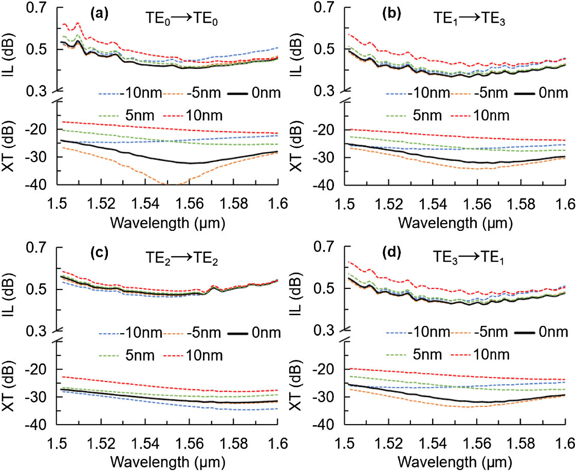
Fig. 4. Simulated spectra of the cross-connected converter with no voltages applied to the electrode heaters for four different input modes. The dotted lines represent the simulated results with different fabrication errors.
3. DEVICE FABRICATION AND RESULTS
To experimentally evaluate the performance of the mode converter, we designed and fabricated a four-mode reconfigurable MDM system on an SOI platform. An electron-beam lithography (Vistec EBPG 5000 Plus) is used to define the patterns, and a single-step inductively coupled plasma dry-etching (Plasmalab System 100) process is used to transfer the mask to the silicon device layer. A 1.2-μm-thick layer is deposited on the silicon layer by plasma-enhanced chemical vapor deposition (PlasmaPro 800 Stratum PECVD). Then a 200-μm-long and 4-μm-wide titanium layer is coated on the branches as micro-heaters by electron beam evaporation (Ebeam-500S). Finally, NiAu electrodes are fabricated for thermal tuning. Figure 5(b) shows the top-view microscope images of the fabricated structure. The detailed scanning electron microscope (SEM) pictures of the fabricated subwavelength four- and dual-mode symmetric Y-junctions and the single-mode waveguide crossing are illustrated in Figs. 5(e)–5(g), respectively. One auxiliary mode multiplexer (MUX) and one de-multiplexer (DEMUX) are connected to the two ends of the converter for the purpose of performance characterization. Several structures have been utilized to realize MUX/DEMUX, such as an MMI [27], asymmetrical directional coupler [10], and asymmetric Y-junction [12]. The cascaded subwavelength asymmetric Y-junctions [26] were employed to excite the higher-order modes in our systems. An extra waveguide with a length of , and an extra waveguide crossing are introduced in the upper/lower branches to balance the initial phase difference, respectively. We also fabricated an extra reference MDM system on the same chip, and it has the same input/output grating couplers and MUX/DEMUX, but without the mode converter, presented in Fig. 5(a). By subtracting the spectra of the reference system, the normalized transmission profiles of the converter could be obtained. The measured average ILs of the mode MUX for , , , and are about 1.12 dB, 1.05 dB, 0.89 dB, and 1.33 dB, respectively, over a wavelength span from 1.53 μm to 1.59 μm. And the measured average XTs among all channels for the four modes are , , , and , respectively.
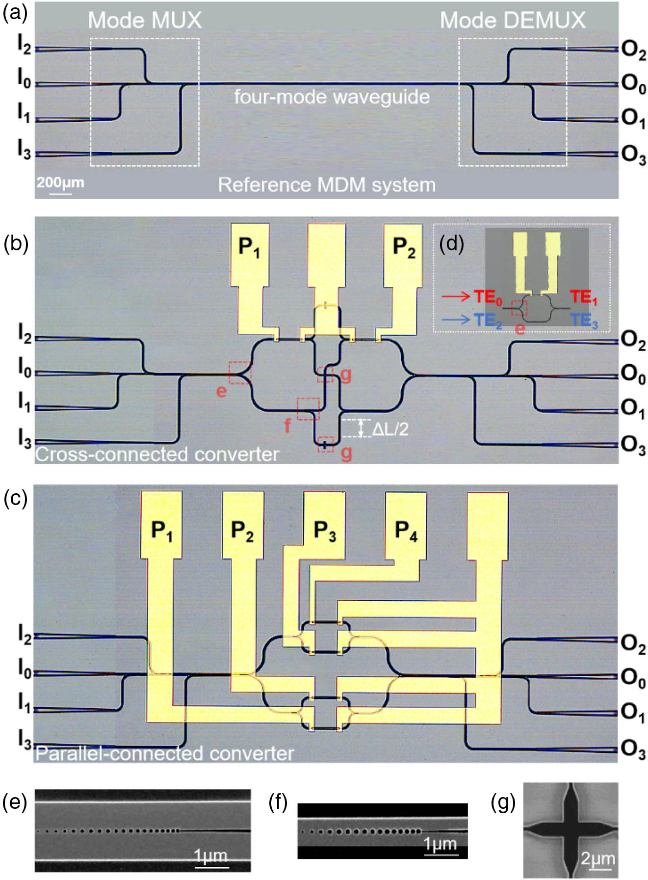
Fig. 5. (a) Optical microscopic image of the reference MDM system. The optical microscopic image of the reconfigurable four-mode MDM systems consisted of (b) cross- and (c) parallel-connected converters; (d) the reference system to determine the power to produce a
A broadband amplified spontaneous emission light source and an optical spectrum analyzer (Yokogawa AQ6370C) were used to characterize the performances of the fabricated devices. The , , , and modes are excited when the light is launched at input ports , , , and , respectively. Optical signals from one input port can be converted to arbitrary output ports by modulating the voltage applied to the NiAu electrodes. We fabricated a reference system to determine the electrical power required for P1 or P2 to produce a -phase change. As shown in Fig. 5(d), it includes two symmetric-connected four-mode symmetric Y-junctions, which allow conversion between TE0 and TE1 modes, or TE2 and TE3 modes. The powers used to produce a -phase change for TE0 and TE1 modes are found to be 37.7 mW and 34.3 mW, respectively. Take the at input port as an example. The signal is converted to the mode at output port when the power applied to and is 37.2 mW and 36.7 mW, respectively, with a total power consumption of 73.9 mW, as shown in Fig. 6(a). Due to the fabrication imperfection, the initial phase differences between the four branches are different, so the corresponding power consumptions applied to P1 and P2 are slightly different from those in Fig. 5(d). Its normalized measured IL and XT profiles are shown in Fig. 6(b). The average IL is 1.97 dB over a wavelength span from 1.53 μm to 1.59 μm. The sum of the transmission spectra measured from the output ports , , and , represents the XT, as the bold red line shown in Fig. 6(b). The measured average XT is . Moreover, the signal is propagated to output port without conversion when the and heating powers are 4.71 and 3.74 mW, and the measured average IL and XT are about 1.9 dB and , respectively. When the applied heating powers to and are 36.5 and 3.4 mW, the signal is converted to the mode at output port with average IL and XT of 1.98 dB and . Similarly, the signal is converted to the mode at output port when the and powers are 0.4 and 36.8 mW, and the average IL and XT are about 1.98 dB and , respectively. Their normalized measured IL and XT profiles are presented in Fig. 6(c). Optical signals from other input ports are also measured in Figs. 6(d)–6(f). The minimum and maximum average ILs of the device are 1.71 dB and 2.45 dB, while the minimum and maximum average XTs are –19.4 dB and –16.6 dB, respectively. The measured ILs are slightly larger than the simulated results in Figs. 4(a)–4(d), which is possibly caused by the etching roughness of waveguides and holes. Further improvement of the ILs could be achieved by reducing the etching roughness via thermal oxidation or hydrofluoric acid removal.
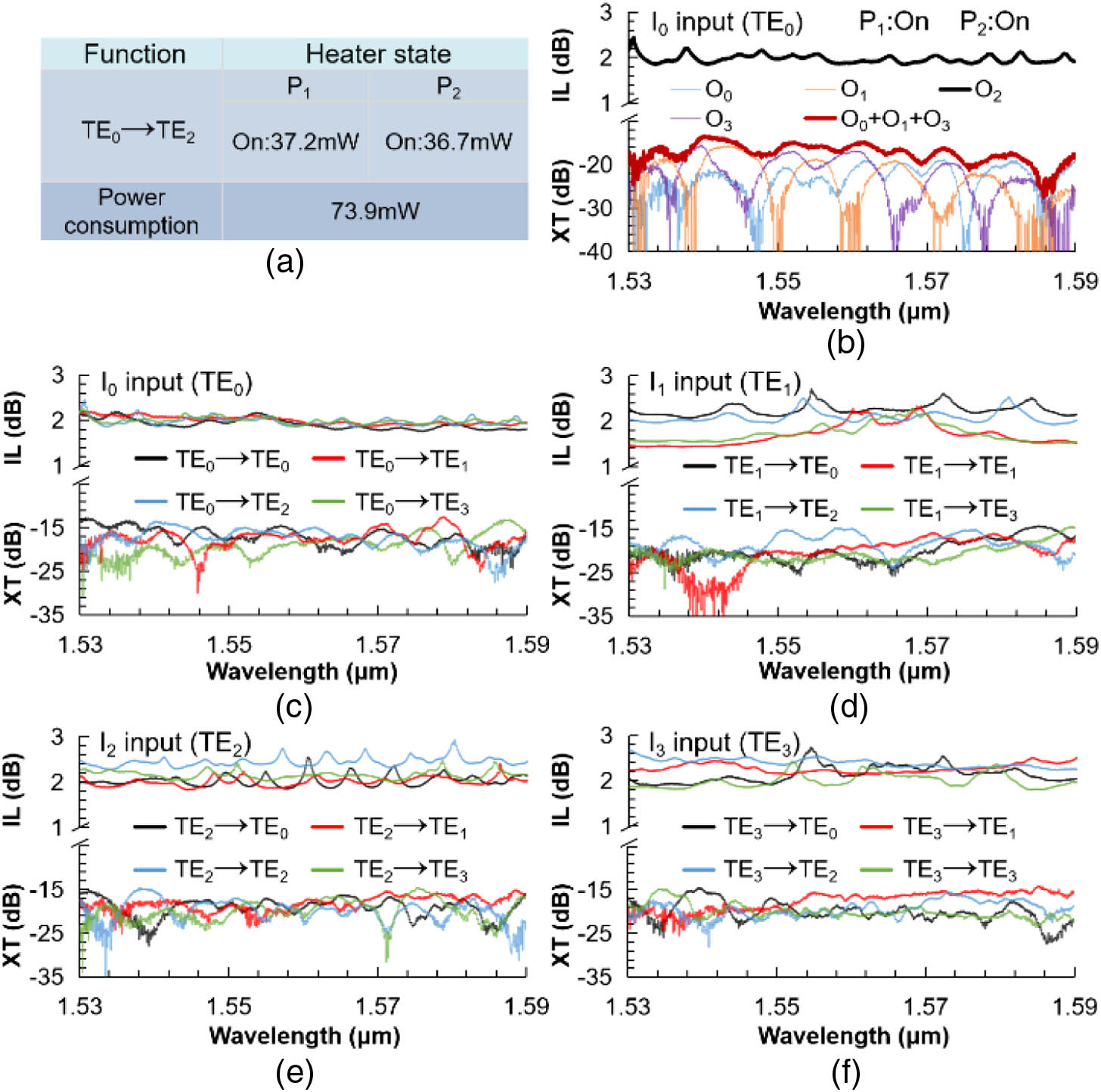
Fig. 6. (a) States of the phase shifters and the power consumption in a specific conversion function. (b) The normalized IL and XT profiles of the converter measured with the
For comparison, we also designed and fabricated a same MDM system in which parallel-connected subwavelength symmetric Y-junctions are used instead. As depicted in Fig. 5(c), four micro-heaters are directly deposited on the four branches, respectively. There are 16 conversion functions for both thermo-optic devices. Figure 7 shows the measured average IL, average XT, and the power consumption profiles for different conversion functions for both cross- and parallel-connected converters, respectively. The minimum and maximum average ILs of the cross-connected one are 1.71 dB and 2.45 dB, respectively. While the minimum and maximum average XTs are and , respectively. For the parallel-connected one, its minimum and maximum average ILs are 1.56 dB and 1.91 dB, and its average XTs are and , respectively. For the cross-connected structure, the number of electrode heaters is reduced by half. By this way the power consumption can be reduced at the expense of sacrificing the IL and XT performance in some cases. For example, the average (IL, XT) of the conversion between the mode and the mode for the parallel-connected one is , with a power consumption of 73.8 mW. For the cross-connected structure, the average (IL, XT) is while consuming only 36.4 mW power. Furthermore, we can even obtain the conversion between the mode and the mode with less than 10 mW power. The IL of the cross-connected converter is slightly larger than that of the parallel one, which may be due to the additional loss introduced by the MMI and bent waveguides. We also compared the average power consumptions of the 16 conversion functions for cross- and parallel-connected converters, respectively. The data presented in the inset of Fig. 7 clearly shows that the average power consumption of the proposed cross-connected converter is smaller than that of the parallel-connected one.
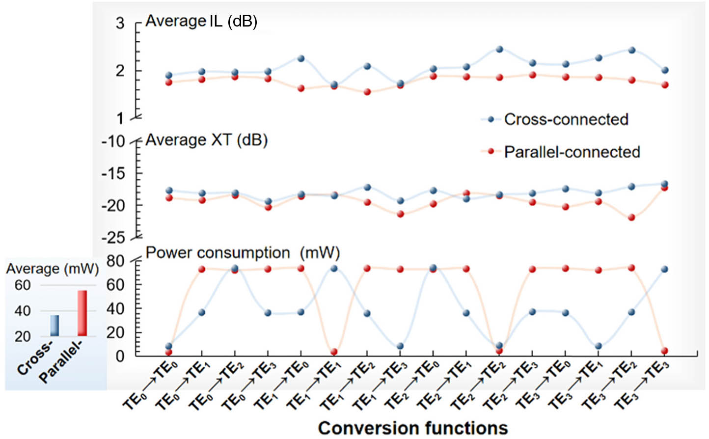
Fig. 7. Measured average ILs, average XTs, and power consumptions for all different conversion functions of cross- and parallel-connected converters, respectively. The inset is the average power consumptions of the 16 conversion functions for cross- and parallel-connected converters.
4. CONCLUSION
In conclusion, we propose and experimentally demonstrate a single-step-etched mode converter toward reconfigurable mode-division multiplexing applications. The mode converter is based on cross-connected subwavelength symmetric Y-junctions assisted by thermo-optic phase shifters. To demonstrate the salient features of the proposed structure, we have designed and fabricated a four-mode device to achieve arbitrary conversions among the first four TE waveguide modes, with only two heating electrodes. Our fabricated device offers the minimum and maximum average (IL, XT) among all different conversions at and , respectively, over a wavelength span from 1.53 μm to 1.59 μm. By reducing the number of micro-heaters, the power consumption of the reconfigurable converter is considerably reduced while the performance of the device is maintained. To the best of our knowledge, it is the first experimental demonstration on an SOI platform of a reconfigurable mode converter supporting up to four modes. The structure can be scalable for even more modes by using an -mode () subwavelength symmetric Y-junction. The thermal tuning process is inherently limited to submillisecond response speed. It is foreseeable that when the mode converter is integrated with plasma-dispersion-based or 2D material-loaded phase shifters [28,29], higher-speed operation (up to nanosecond response time) can be achieved, which is critical for future low-power, high-speed, mode-division multiplexing integrated optical networks.
[1] A. Shacham, K. Bergman, L. P. Carloni. Photonic networks-on-chip for future generations of chip multiprocessors. IEEE Trans. Comput., 2008, 57: 1246-1260.
[2] D. A. B. Miller. Device requirements for optical interconnects to silicon chips. Proc. IEEE, 2009, 97: 1166-1185.
[3] W. Shipeng, F. Xianglian, G. Shiming, S. Yaocheng, D. Tingge, Y. Hui. On-chip reconfigurable optical add-drop multiplexer for hybrid wavelength/mode-division-multiplexing systems. Opt. Lett., 2017, 42: 2802-2805.
[4] J. Wang, S. He, D. Dai. On-chip silicon 8-channel hybrid (de)multiplexer enabling simultaneous mode- and polarization-division-multiplexing. Laser Photonics Rev., 2014, 8: L18-L22.
[5] L. W. Luo, N. Ophir, C. P. Chen, L. H. Gabrielli, C. B. Poitras, K. Bergmen, M. Lipson. WDM-compatible mode-division multiplexing on a silicon chip. Nat. Commun., 2014, 5: 3069.
[6] D. Dai, J. E. Bowers. Silicon-based on-chip multiplexing technologies and devices for peta-bit optical interconnects. Nanophotonics, 2014, 3: 283-311.
[7] W. Chang, L. Lu, X. Ren, D. Li, Z. Pan, M. Cheng, D. Liu, M. Zhang. Ultra-compact mode (de)multiplexer based on subwavelength asymmetric Y-junction. Opt. Express, 2018, 26: 8162-8170.
[8] D. Dai. Silicon nanophotonic integrated devices for on-chip multiplexing and switching. J. Lightwave Technol., 2017, 35: 572-587.
[9] L. Yang, T. Zhou, H. Jia, S. Yang, J. Ding, X. Fu, L. Zhang. General architectures for on-chip optical space and mode switching. Optica, 2018, 5: 180-187.
[10] D. Dai, J. Wang, Y. Shi. Silicon mode (de)multiplexer enabling high capacity photonic networks-on-chip with a single-wavelength-carrier light. Opt. Lett., 2013, 38: 1422-1424.
[11] Y. Ding, J. Xu, F. Da Ros, B. Huang, H. Ou, C. Peucheret. On-chip two-mode division multiplexing using tapered directional coupler-based mode multiplexer and demultiplexer. Opt. Express, 2013, 21: 10376-10382.
[12] W. Chen, P. Wang, J. Yang. Mode multi/demultiplexer based on cascaded asymmetric Y-junctions. Opt. Express, 2013, 21: 25113-25119.
[13] D. Dai, Y. Tang, J. E. Bowers. Mode conversion in tapered submicron silicon ridge optical waveguides. Opt. Express, 2012, 20: 13425-13439.
[14] L. H. Frandsen, Y. Elesin, L. F. Frellsen, M. Mitrovic, Y. Ding, O. Sigmund, K. Yvind. Topology optimized mode conversion in a photonic crystal waveguide fabricated in silicon-on-insulator material. Opt. Express, 2014, 22: 8525-8532.
[15] H. Jia, T. Zhou, X. Fu, J. Ding, L. Yang. Inverse-design and demonstration of ultracompact silicon meta-structure mode exchange device. ACS Photonics, 2018, 5: 1833-1838.
[16] Q. Zhang, Y. Zhang, J. Li, R. Soref, T. Gu, J. Hu. Broadband nonvolatile photonic switching based on optical phase change materials: beyond the classical figure-of-merit. Opt. Lett., 2018, 43: 94-97.
[17] H. Chen, H. Jia, J. Yang, Y. Tian, T. Wang. Ultra-compact switchable mode converter based on silicon and optical phase change material hybrid metastructure. Opt. Commun., 2020, 473: 125889.
[18] X. Han, Z. Zhang, J. Yang, H. Xiao, Y. Tian. On-chip switchable and reconfigurable optical mode exchange device using cascaded three-waveguide-coupling switches. Opt. Express, 2020, 28: 9552-9562.
[19] C. Sun, Y. Yu, G. Chen, X. Zhang. Integrated switchable mode exchange for reconfigurable mode-multiplexing optical networks. Opt. Lett., 2016, 41: 3257-3260.
[20] Q. Huang, W. Jin, K. S. Chiang. Broadband mode switch based on a three-dimensional waveguide Mach-Zehnder interferometer. Opt. Lett., 2017, 42: 4877-4880.
[21] L. B. Soldano, E. C. M. Pennings. Optical multi-mode interference devices based on self-imaging: principles and applications. J. Lightwave Technol., 1995, 13: 615-627.
[22] R. Liu, L. Lu, P. Zhang, W. Chang, M. Zhang. Integrated dual-mode 3 dB power splitter based on multimode interference coupler. IEEE Photonics Technol. Lett., 2020, 32: 883-886.
[23] N. Riesen, S. Gross, J. Love, M. J. Withford. Femtosecond direct-written integrated mode couplers. Opt. Express, 2014, 22: 29855-29861.
[24] J. Dong, K. S. Chiang, W. Jin. Mode multiplexer based on integrated horizontal and vertical polymer waveguide couplers. Opt. Lett., 2015, 40: 3125-3128.
[25] C. Sun, Y. Yu, X. Zhang. Ultra-compact waveguide crossing for a mode-division multiplexing optical network. Opt. Lett., 2017, 42: 4913-4916.
[26] L. Lu, D. Liu, M. Yan, M. Zhang. Subwavelength adiabatic multimode Y-junctions. Opt. Lett., 2019, 44: 4729-4732.
[27] T. Uematsu, Y. Ishizaka, Y. Kawaguchi, K. Saitoh, M. Koshiba. Design of a compact two-mode multi/demultiplexer consisting of multimode interference waveguides and a wavelength-insensitive phase shifter for mode-division multiplexing transmission. J. Lightwave Technol., 2012, 30: 2421-2426.
[28] G. T. Reed, G. Mashanovich, F. Y. Gardes, D. J. Thomson. Silicon optical modulators. Nat. Photonics, 2010, 4: 518-526.
[29] V. Sorianello, M. Midrio, G. Contestabile, I. Asselberghs, J. Van Campenhout, C. Huyghebaert, I. Goykhman, A. K. Ott, A. C. Ferrari, M. Romagnoli. Graphene-silicon phase modulators with gigahertz bandwidth. Nat. Photonics, 2018, 12: 40-44.
Article Outline
Longhui Lu, Deming Liu, Max Yan, Minming Zhang. On-chip reconfigurable mode converter based on cross-connected subwavelength Y-junctions[J]. Photonics Research, 2021, 9(1): 01000043.
