Matter and Radiation at Extremes, 2020, 5 (1): 018201, Published Online: Feb. 18, 2020  

Pressure responses of halide perovskites with various compositions, dimensionalities, and morphologies Download: 501次

Author Affiliations
Center for High Pressure Science and Technology Advanced Research (HPSTAR), Shanghai 201203, China
Abstract
Metal halide perovskites (HPVs) have been greatly developed over the last decade, with various compositions, dimensionalities, and morphologies, leading to an emergence of high-performance photovoltaic and optoelectronic applications. Despite the tremendous progress made, challenges remain, which calls for a better understanding of the fundamental mechanisms. Pressure, a thermodynamic variable, provides a powerful tool to tune materials’ structures and properties. In combination with in situ characterization methods, high-pressure research could provide a better fundamental understanding. In this review, we summarize the recent studies of the dramatic, pressure-induced changes that occur in HPVs, particularly the enhanced and emergent properties induced under high pressure and their structure-property relationships. We first introduce the characteristics of HPVs and the basic knowledge of high-pressure techniques, as well as in situ characterization methods. We then discuss the effects of pressure on HPVs with different compositions, dimensionalities, and morphologies, and underline their common features and anomalous behaviors. In the last section, we highlight the main challenges and provide suggestions for possible future research on high-pressure HPVs.

1 I. INTRODUCTION

In the past several years, photovoltaic devices based on halide perovskites (HPVs) have made impressive progress in their development, attaining energy conversion efficiencies of over 25%, surpassing the already commercialized polysilicon, cadmium telluride, and copper indium gallium selenide photovoltaic devices.1–4 Furthermore, HPVs have also shown great potential in optoelectronics, including in light-emitting diodes,5–8 photodetectors,9 and lasers.10,11 Their outstanding photovoltaic and optoelectronic functionalities have been attributed to their superior electronic and optical properties, such as long charge diffusion distances, small carrier effective masses, and high optical absorption coefficients.12–15 These excellent characteristics, along with low fabrication cost, motivate further intense study for both theoretical and technological reasons.16 Moreover, the rapid development of HPVs for energy-related applications does not only stem from their outstanding functionalities but also from the substantial adjustability of their crystalline structures and dimensionalities.

Despite their unique properties and impressive achievements, inherent challenges remain in HPVs that need to be addressed, calling for a better understanding of the mechanisms that dominate their outstanding functionalities. The soft lattices of HPVs render them sensitive to mechanical compression, which can effectively adjust their atomic and electronic structures, as well as their physical properties, without changing their chemical composition. In combination with various in situ characterization probes, high-pressure research could further our fundamental understanding of the structure-property relationship. As a fundamental parameter, pressure can efficiently adjust the structures of materials, leading to exceptional enhancements from external dimensional tuning. In this review, we summarize the recent progress made in the research of pressure-induced changes in the structures and properties of HPVs. We begin by introducing the characteristics of HPVs and the fundamental knowledge of high-pressure techniques together with in situ characterizations. We then discuss the effects of pressure on HPVs with different compositions, dimensionalities, and morphologies, focusing on the enhanced and emergent properties induced by high-pressure treatment, as well as the structure-property relationship. The final section highlights the main challenges and outlook of high-pressure research on HPVs.

1.3 A. Crystal structures and physical properties of HPVs

Perovskite is a class of materials that has the general formula ABX3.17 As shown in Fig. 1(a), cation “B” has six nearest-neighbored anions “X,” and cation “A” occupies a vacancy formed by eight corner-sharing [BX6]4− octahedrons.18,19 In the case of HPVs, typically an “A” site can be occupied by either an inorganic ion (e.g., Cs+) or an organic ion [e.g., CH3NH3+ (MA), NH2CH = NH2+ (FA)], thereby generating different types of HPVs; “B” is a divalent metal cation (e.g., Pb2+, Sn2+, or Ge2+) and “X” is a halide anion (e.g., Cl, Br, or I). The crystal symmetry and phase stability of the perovskite structure can be determined using the Goldschmidt’s tolerance factor t=(RA+RB)/2(RB+RX) and an octahedral factor m = RB/RX. The tolerance factor (t) is defined as the ratio of the distances between A–X and B–X in the idealized rigid-body ball model, where RA, RB, and RX are the ionic radii of A, B, and X ions, respectively.20 In organic–inorganic HPVs, a stable structure can exist with 0.81 < t < 1.11 and 0.44 < m < 0.90. If the tolerance factor is in the range of 0.9–1.0, a cubic structure is expected, while different values give less-symmetric crystal structures. Figure 1(b) shows t of different HPVs.21

Fig. 1. (a) Schematic diagram of perovskite structure. This figure is reproduced with permission from Yin et al., J. Mater. Chem. A 3, 8926–8942 (2015). Copyright 2015 The Royal Society of Chemistry.28 (b) Tolerance factors (t) for different organic–inorganic HPVs. This figure is reproduced with permission from Fan et al., J. Mater. Chem. A 3, 18809–18828 (2015). Copyright 2015 The Royal Society of Chemistry.21 (c) Crystal structures of 3D and 2D HPVs. This figure is taken from Ref. 27. (d) Crystal structures of the 2D HPV of L2An-1BnX3n+1 (from n = 1 to n = ∞) with different [BX6]4− octahedral layers. The number of inorganic layers n = ∞ corresponds to 3D HPV structure. (c) and (d) Reproduced with permission from Jaffe et al., ACS Energy Lett. 2, 1549–1555 (2017). Copyright 2017 American Chemical Society.27

下载图片 查看所有图片

The earliest research conducted on organic–inorganic lead HPVs (e.g., MAPbX3, X = Cl, Br, and I) mainly focused on their outstanding photovoltaic performance. All inorganic compounds (e.g., CsPbX3) then became attractive because of their high stability and tunable functionalities. Both theoretical and experimental evidence has shown that the three elements of A, B, and X in the ABX3 crystalline structure can be chemically substituted, resulting in a series of mixed compounds.22,23 In addition, two divalent B2+ cations can be replaced by a trivalent cation and a monovalent cation to form a quaternary halide with a dual perovskite structure.10 This strategy has been used to explore novel lead-free double perovskites, for example, using Ag+ and Bi3+ cations to replace two Pb2+ cations.24

More recently, the reduced-dimensional HPVs, especially two-dimensional (2D) layered perovskite materials, have given rise to a very diverse semiconductor subgroup with high tunability and eminently adjustable photophysical properties.8,25 Ruddlesden–Popper (RP) HPVs can be imagined as molecular sheets inserted into a three-dimensional (3D) structure in one direction, which can be described as L2An-1BnX3n+1, where A represents cations in the voids among the octahedra (e.g., CH3NH3+), L represents organic cations between different layers, and n is the number of metal halide octahedral layers between insulating L organic layers.26 The 2D structure consists of a single-layer or a multilayer [BX6]4− octahedral sheet [An-1BnX3n+1]2− separated by L cations, and thus the 3D perovskite framework is reduced to a 2D structure due to steric hindrance [Fig. 1(c)].27 The obtained 2D compounds possess a structure of alternating organic and inorganic layers, with adjacent organic layers interacting through weak van der Waals interactions. Figure 1(d) shows examples of RP-type HPVs. Due to their unique structure, 2D HPVs exhibit better stability and higher adjustability.

HPVs are typically direct bandgap materials with high optical absorption coefficients. The bandgap of a semiconductor determines the absorption width of the solar spectrum, and HPVs exhibit a bandgap ranging from about 1 to 3 eV. For 3D HPVs, most of their bandgap edges consist of orbitals from metal B and halogen X.29 Their valence band maximum (VBM) usually consists of both np6 orbitals from X (n is the principal quantum number, n = 5, 4, and 3 for I, Br, and Cl, respectively) and ns2 orbitals from B (n = 6, 5, and 4 for Pb, Sn, and Ge, respectively). The conduction band minimum (CBM) mostly consists of the empty np0 orbital from B.20 The orbitals of A in HPVs structure are far from the band edges, so their direct contribution to the bandgap is negligible.30 However, A cations affect the lattice constants, which indirectly influence band structure. In addition, A cations can affect inorganic octahedral distortion, dielectric constants, and hydrogen bonding.31 Qualitatively, the band structure of the perovskites is strongly dependent on crystallographic symmetry.32 Different from the 3D HPV analogs, 2D HPVs have less size constrict for the L-sites (A-sites comply with the same rules as 3D HPVs). Organic cations can not only act as an insulating barrier that confines the charge carriers in the 2D plane, but also as dielectric regulators that determine the electrostatic forces applied to the carriers.

The interaction among metal-halide units in 3D HPVs results in the formation of electron bands that have large bandwidths. In addition to possessing a long distance for carrier transport, HPVs absorb a wide range of wavelengths, possessing a high absorption coefficient, producing an outstanding photovoltaic performance.33 Different from the 3D compounds, the special arrangement of alternating organic–inorganic layers of 2D HPVs produces crystal-ordered 2D quantum wells that exhibit strong structural distortion and significant quantum confinement effects, giving rise to the formation of free excitons and trapped excited states during photoexcitation.33–35

The bandgaps of the materials can be optimized by different methods, influencing optoelectronic performance. One possible way to adjust the bandgap of the material is to change the chemical composition or doping of the material, such as by changing the proportion of constituent halides. The mixed-cation HPVs with lead and tin at the B sites can also reduce the bandgap, but this shortens their carrier lifetime and compromises their stability.10,36–38 However, mechanical compression provides another way to effectively adjust the structures and properties. The relatively soft lattices of HPVs render them suitable for high-pressure investigations, which can not only enhance our fundamental understanding of them but also allow us to extract from them emergent and enhanced properties. The application of external pressure can cause dramatic changes in both the structural and physical properties of HPVs, including the shrinkage and titling of [BX6]4− octahedra, lattice disordering, bandgap closing, and carrier lifetime modification.39 Furthermore, as ions A, B, and X usually have different compressibilities, the tolerant factors t change as a function of applied pressure, which leads to improved structure and electronic tunability.

1.4 B. Basic knowledge of high-pressure science and technology

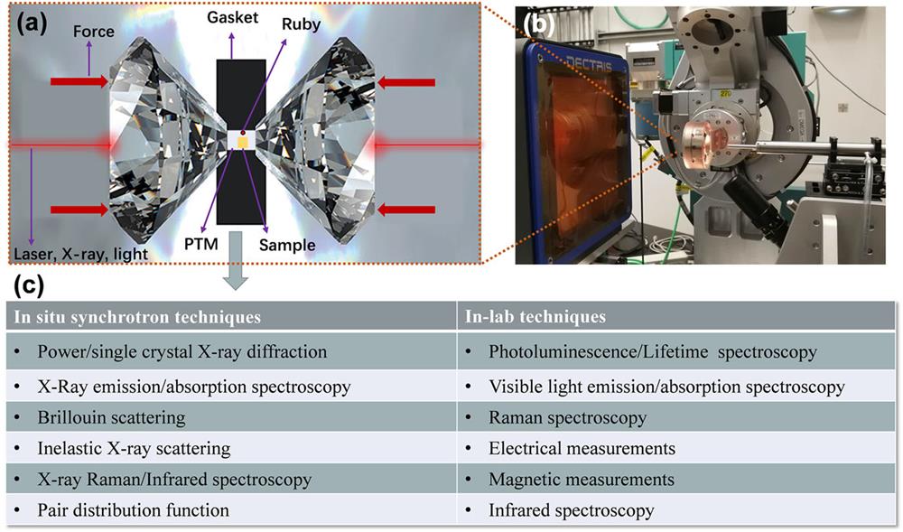
As a thermodynamic parameter, pressure can be employed to tune the properties of materials by adjusting their interatomic distances, electronic orbitals, and bonding patterns.40–43 The static compression realized by diamond anvil cells (DACs) has produced attainable pressures of up to hundreds of gigapascals (1 GPa = 10 000 atm).13,44 DACs [Fig. 2(a)], with a pair of diamond anvils in opposing geometry, are used to compress samples immersed in a pressure transmitting media (PTM), like silicone oil, neon, and helium. At room temperature, helium solidifies at about 11 GPa, which provides the best hydrostatic-pressure conditions under high pressure. Diamond is a material with excellent transparency to a very wide range of electromagnetic radiation, making it attractive for in situ synchrotron, x-ray, and in-laboratory optical probes [Figs. 2(b) and 2(c)]. Furthermore, in situ electrical transport, photocurrent, and magnetic susceptibility measurements have also been developed within DACs.

Fig. 2. (a) Schematic diagram of the sample in a DAC. (b) High-pressure synchrotron-based setup for diffraction. (c) In situ in-laboratory and synchrotron-based characterization tools under high pressures.

下载图片 查看所有图片

In the last several years, the previously small field of high-pressure science and technology has grown significantly, becoming increasingly attractive to the physics, chemistry, and materials sciences communities.27,32,45–52 Combing in-laboratory and synchrotron-based characterization methods, one may elucidate many interesting phenomena, as well as explore novel materials with enhanced and emergent properties, which are inaccessible at ambient pressures. Moreover, high-pressure synchrotron-based techniques have developed rapidly, greatly contributing to high-pressure research in physics, chemistry, and materials sciences40,53,54 in various forms: x-ray diffraction (XRD) characterizes long-range crystal structure; x-ray emission spectroscopy provides information on electronic states; nuclear resonant x-ray spectroscopy examines phonon densities of state; x-ray Raman spectroscopy monitors changes in chemical bonding; the pair distribution function (PDF) reveals local bonding features at the atomic scale; and x-ray imaging examines internal strain, hierarchical structure, and dynamic processes.32 By combining these synchrotron-based characterization tools with in-laboratory physical property measurement methods, including absorption spectroscopy, photoluminescence (PL), and photocurrent and electrical transport measurements, one can monitor the structural, optical, electrical, and optoelectronic properties in situ under high pressure.55 By enabling new structures and properties, high pressure might not only offer new opportunities to explore novel materials, but might also introduce new ways to study structure-property relationships. Note that the high-pressure results reported by different research groups are sometimes inconsistent.56 This discrepancy is possibly due to the different high-pressure methods used, as well as varying experimental conditions. A particularly important aspect is the pressure condition, including pressure anisotropy, strain levels, and gradients, which are determined by the pressure transmitting media and pressure-loading dynamics.57 Poor hydrostatic conditions result in higher deviatoric stresses that typically facilitate or even change pressure-induced transition processes.

The study of HPVs under high pressure can be traced back to the 1990s and focused on their P-T phase diagrams of MAPbX3.58 Intense focus has been on HPVs since they delivered outstanding performances in photovoltaic applications.2,10,59–67 In recent years, high-pressure research in HPVs materials has produced increasing numbers of new discoveries and phenomena.52,68–76 Several scientific review papers have focused on HPVs under high pressure,15,27,39,47,48,77–80 but a comprehensive review addressing the recent high-pressure discoveries regarding HPVs has remained rare. Here, we summarize the pressure effects on the lattice and the electronic, optical, and electrical properties of HPVs, with different compositions, dimensionalities, and morphologies. We focus on the enhanced and emergent properties induced by high-pressure treatment. High-pressure studies on the structural and physical properties of HPVs provide valuable clues for the further optimization of these materials, helping to extract enhanced performances and provide experimental baselines for theoretical modeling.

2 II. PRESSURE-TUNED AND PRESSURE-ENHANCED PROPERTIES

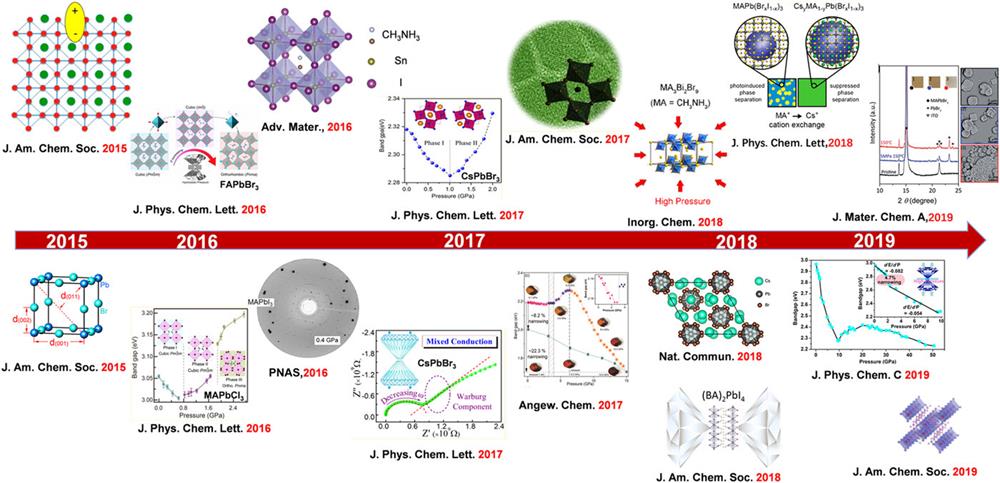
In general, pressure-induced shortening of the bond length narrows the bandgap while bending of the B–X–B angle widens it.81 Effective tuning of the structures under high pressure leads to changes in their original nature and can produce emergent properties. In the past several years, research on the high-pressure behavior of HPVs has achieved unprecedented rapid development.5,6,11,20,33,37,43,54,57,70,82–87 As shown in Fig. 3, gratifying achievements in comprehensive analysis, including that related to pressure-induced variations in crystal structure, PL, electrical resistance, and photocurrent, have been increasingly reported (Fig. 3). In this section, we have summarized the pressure-induced structural evolution and property improvements of HPVs, with various compositions, dimensionalities, and morphologies.

Fig. 3. The research progress of HPVs under high pressure. Reproduced with permission from Wu et al., J. Am. Chem. Soc. 137, 2089–2096 (2015). Copyright 2015 The Royal Society of Chemistry;33 Wang et al., J. Am. Chem. Soc. 137, 11144–11149 (2015). Copyright 2015 The Royal Society of Chemistry;54 Wang et al., J. Phys. Chem. Lett. 7, 2556–2562 (2016). Copyright 2016 The Royal Society of Chemistry;86 Wang et al., J. Phys. Chem. Lett. 7, 5273–5279 (2016). Copyright 2016 The Royal Society of Chemistry;87 Lu et al., Adv. Mater. 28, 8663–8668 (2016). Copyright 2016 Wiley-VCH Verlag GmbH & Co. KGaA;37 Kong et al., Proc. Natl. Acad. Sci. 113, 8910–8915 (2016);82 Zhang et al., J. Phys. Chem. Lett. 8, 3752–3758 (2017). Copyright 2017 The Royal Society of Chemistry;84 Yan et al., J. Phys. Chem. Lett. 8, 2944–2950 (2017). Copyright 2017 The Royal Society of Chemistry;70 Xiao et al., J. Am. Chem. Soc. 139, 10087–10094 (2017). Copyright 2017 The Royal Society of Chemistry;43 Wang et al., Angew. Chem., Int. Ed. 56, 15969–15973 (2017). Copyright 2017 Wiley-VCH Verlag GmbH & Co. KGaA;83 Zhu et al., Inorg. Chem. 57, 6206–6209 (2018). Copyright 2018 The Royal Society of Chemistry;6 Ma et al., Nat. Commun. 9, 4506 (2018). Copyright 2018 Springer Nature;11 Bischak et al., J. Phys. Chem. Lett. 9, 3998–4005 (2018). Copyright 2018 The Royal Society of Chemistry;5 Ding et al., J. Mater. Chem. A 7, 540–548 (2019). Copyright 2019 The Royal Society of Chemistry;20 Ren et al., J. Phys. Chem. C 123, 15204–15208 (2019). Copyright 2019 The Royal Society of Chemistry;88 and Shi et al., J. Am. Chem. Soc. 141, 6504–6508 (2019). Copyright 2019 The Royal Society of Chemistry.85

下载图片 查看所有图片

2.3 A. 3D organic–inorganic HPVs

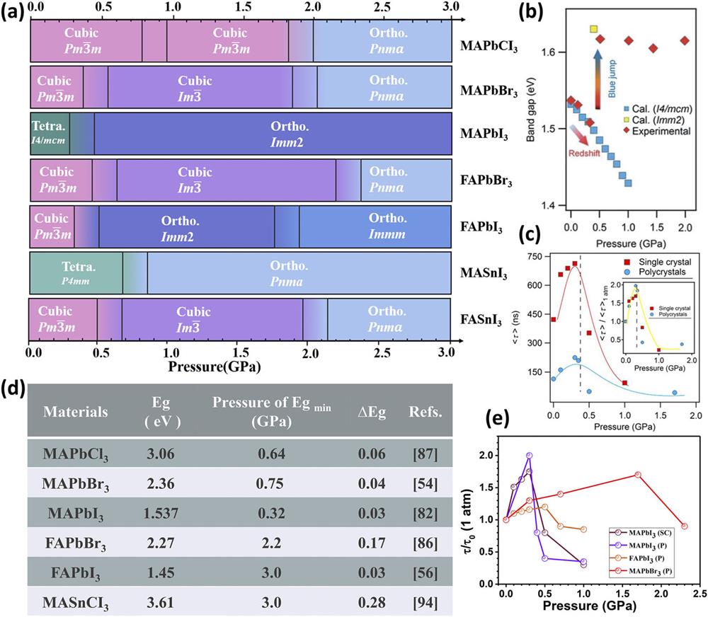
3D organic–inorganic HPVs are the type studied most and they exhibit the best photovoltaic performance. In particular, the electronic structures and optical properties of MAPbX3 under pressure have been experimentally and theoretically investigated.55,89–92 It has been reported that organic–inorganic HPVs exhibit cubic, tetragonal, and orthorhombic phases under different temperatures and pressures. The cubic structure typically possesses a wider electronic band, showing a smaller effective mass and higher mobility. The lower symmetry of tetragonal and orthogonal structures under different temperatures provides some references for the understanding of pressure-induced structural evolution. Wang et al. reported that MAPbCl3 shows pressure-induced structural evolution, as in the following: Pm3¯m (1 atm) → Pm3¯m (0.8 GPa) → Pnma (2.4 GPa). The transformation from phase І to phase Ⅱ is attributed to the cubic–cubic isostructural phase transition [Fig. 4(a)].87 The cubic Pm3¯m MAPbBr3 transforms to Im3¯ at 0.4 GPa, further to Pnma at 1.8 GPa, then starts amorphization at 2 GPa, reverting to the original crystalline structure upon decompression [Fig. 4(a)].54 Capitani et al. reported that MAPbI3 transforms from tetragonal I4/mcm at ambient pressure to orthorhombic Imm2 at 0.26 GPa, undergoing gradual amorphization at above 3 GPa [Fig. 4(a)].90 Similar high-pressure behavior has been reported for the FA based compounds. In particular, the structural change in the FAPbBr3 crystal exhibits a similar pressure-induced phase transition to MAPbBr3 but requires higher pressures: Pm3¯m (1 atm) → Im3¯ (0.53 GPa) → Pnma (2.2 GPa) → amorphization (4.1 GPa) [Fig. 4(a)].86 The pressure points corresponding to the structural transitions of FAPbBr3 are higher than those of MAPbBr3 crystal, which means that the former is less compressible. It is reported that FAPbI3 shows the following structural evolution under pressure Pm3¯m (1 atm) → Imm2 (0.34 GPa) → Immm (1.67 GPa) [Fig. 4(a)].56 Furthermore, Lu et al. reported a lead-free perovskite MASnI3 exhibiting the pressure-driven phase transitions of P4mm (1 atm) → Pnma (0.7 GPa) → amorphization (3 GPa).37 Lee et al. reported that the phase transitions of FASnI3 follow Pm3¯mIm3¯I4/mmm → amorphization [Fig. 4(a)].93

Fig. 4. (a) Summary of pressure-induced structural evolution in MAPb/SnX3. (b) Pressure-induced bandgap evolution of MAPbI3. (c) Pressure dependence of average carrier lifetimes of single crystal and polycrystalline MAPbI3; inset shows normalized results. (b) and (c) Reproduced with permission from Kong et al., Proc. Natl. Acad. Sci. 113, 8910–8915 (2016).82 (d) Comparison of pressure-induced variations of the electronic structure of MA/FAPbX3. These include the bandgap (Eg), the pressure at the minimum bandgap (Egmin), and the bandgap decreased values (∆Eg). These figures are taken from Refs. 54, 56, 82, 86, 87, and 94. (e) Summary of several organic–inorganic HPV carrier lifetimes under high pressure.

下载图片 查看所有图片

It is inevitable that pressure-induced structural transitions lead to variations in bandgaps. According to the so-called Shockley–Queisser theory, the optimum bandgap for solar cells is 1.34 eV, which offers a theoretical power conversion efficiency of 33%. However, the bandgaps of HPVs are normally greater than this ideal value. In situ high-pressure optical measurements, such as absorption spectroscopy and PL spectroscopy, could be used to monitor and understand the bandgap evolution of HPVs. During compression, the electron distribution and orbital interactions within the system can be changed by decreasing interatomic distances, thus adjusting the band structures. For the organic–inorganic HPVs with [BX6]4− octahedra, the pressure response of the bandgaps is between 17 and 100 meV/GPa. Kong et al. achieved a simultaneous evolution of bandgap narrowing (0.03 eV) and PL lifetime prolongation of single MAPbI3 crystals under a pressure of 0.3 GPa.82 Under ambient conditions, the bandgap of MAPbI3 is 1.537 eV. As pressure increases, the bandgap gradually redshifts to 1.507 eV at 0.32 GPa, which is mainly caused by the upshift of VBM due to the shortening of bond length. In addition, a sudden blueshift occurs as pressure further increases, according to the phase transition from tetragonal I4/mcm to orthorhombic Imm2 [Fig. 4(b)]. Time-resolved PL measurements were performed under pressure, which revealed a carrier lifetime prolongation from 425 ns at ambient pressure to 715 ns at 0.3 GPa [Fig. 4(c)], enhanced by ∼70%. The bandgaps of various 3D organic–inorganic HPVs and their relevant parameters are summarized in Fig. 4(d). The enhancement of carrier lifetimes in MAPbI3, MAPbBr3, and FAPbI3, are summarized in Fig. 4(e).

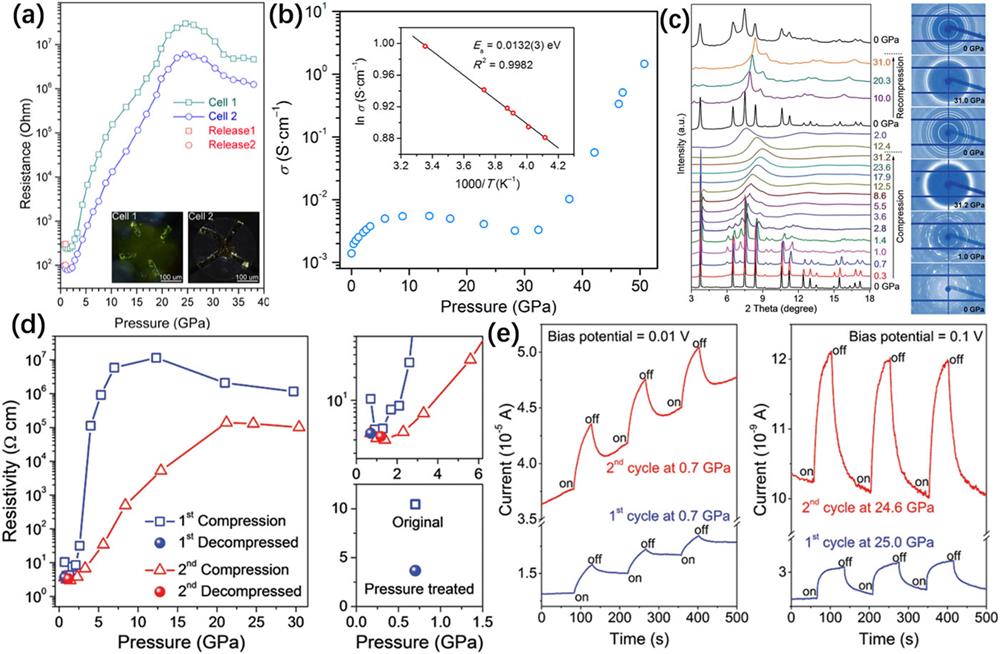
Electrical conductivity and photocurrent are important characteristics for applications in optoelectronic devices. High-pressure studies on the electrical properties of HPVs are critical to revealing structure-property relationships. Wang et al. conducted electrical resistance measurements on MAPbBr3 using a four-probe method within a DAC [Fig. 5(a)].54 The measurements showed a rapid increase in the electrical resistance from 2 to 25 GPa, and the maximum value reached five orders of magnitude larger than the initial value, which may be attributed to pressure-induced amorphization. However, Jaffe et al. reported a distinct behavior of the pressure-induced conductivity change in MAPbI3.91 The conductivity increased during compression and reached a plateau at about 10 GPa, followed by a slight decrease up to 30 GPa. At higher pressures of up to 51 GPa, a significant increase in the conductivity by two orders of magnitude was observed [Fig. 5(b)]. The authors ascribe the sharp increase in electron transport to pressure-induced metallization. It is difficult to explain the distinct behavior in these two studies from two different research groups, and more systematic studies are needed. Ou et al. reported that the photocurrent of FAPbBr3 increased remarkably at 1.3 GPa, and the highest value was nearly ten times higher than that of MAPbBr3, and about three times higher than that of MAPbI3.95

Fig. 5. (a) Electrical resistance as a function of pressure for MAPbBr3. The inset in panel (a) shows microphotographs of the samples with four Au probes in two DACs. This figure is reproduced with permission from Wang et al., J. Am. Chem. Soc. 137, 11144–11149 (2015). Copyright 2015 American Chemical Society.54 (b) Electrical conductivity of MAPbI3 as a function of pressure. Inset shows the Arrhenius fit of the temperature-dependent conductivity at 51 GPa, which gives an activation energy Ea of 13.2(3) meV. This figure is taken from Ref. 91. (c) XRD patterns of MASnI3 under cyclic pressurization and original XRD images at six selected pressures. (d) Pressure-induced evolution of electrical resistivity and comparison of resistivity before and after high-pressure treatment. (e) Photocurrent changes under pressure. The blue line indicates the first loop and the red line indicates the second loop. These figures are reproduced with permission from Lu et al., Adv. Mater. 28, 8663–8668 (2016). Copyright 2016 Wiley-VCH Verlag GmbH & Co. KGaA.37

下载图片 查看所有图片

Lu et al. systematically investigated the differences in the structures and properties of lead-free HPV before and after high-pressure treatments.37 MASnI3 was treated by two sequential compression-decompression cycles at up to 30 GPa. During the first compression process the phase transition sequence is P4mm (1 atm) → Pnma (0.7 GPa) → amorphization (3 GPa). Surprisingly, the crystalline nature of MASnI3 can be maintained during the re-compression process up to 31 GPa [Fig. 5(c)]. Pressure can change the crystal structures and properties of HPVs; however, whether the unique properties generated under high pressures can be retained in the sample upon decompression is a matter of great concern. From this perspective, Lu et al. systematically compared the structural stability, electrical conductivity, and photo responsiveness of lead-free MASnI3 HPV before and after high-pressure treatment, by applying two sequential compression-decompression cycles at up to 30 GPa.37 Remarkably, in situ XRD, Raman spectroscopy, transport, and photocurrent measurements show that the pressure-induced amorphous and recrystallized sample exhibits considerable improvements in structural stability, electron transport, and photo responsiveness [Figs. 5(c)–5(e)]. In the first cycle, the MASnI3 experiences pressure-induced amorphization at about 3 GPa and recrystallizes to a crystalline phase upon pressure release, a typical pressure response in other HPVs.48,84,90 Surprisingly, in the second compression process, no amorphization can be observed above 30 GPa. In situ resistance measurements show that the conductivity of MASnI3 after high-pressure treatment is three-fold higher than the initial value [Fig. 5(d)], which demonstrates higher electron mobility. Ambient pressure photocurrent measurements also disclose a significant enhancement in the photoresponsiveness of MASnI3 after high-pressure treatment [Fig. 5(e)]. Therefore, the optoelectronic properties of the pressure-treated perovskites are considerably enhanced, indicating the significant effects of pressure on HPVs. In addition, Yan et al. reported the electrical transport and photoresponse of MAPbBr3 using in situ alternating-current (AC) impedance spectroscopy and photocurrent measurements.70 Since the electrons and ions have very different responses to varied-frequency AC signals, in situ AC impedance spectroscopy provides an effective way to distinguish between electronic and ionic conduction. The mixed conduction from both ions and electrons was found in MAPbBr3 and an ionic-electronic conduction transition occurred at 3.3 GPa. Combined with the results of structural variation, the conduction transition can be attributed to pressure-induced phase transitions. From the photocurrent measurements, the response to light of the high-pressure phase is obviously superior to that of the initial phases, signifying that pressure is effective in further enhancing the photovoltaic properties of the halide perovskite.

From these high-pressure investigations, one can optimize the performance of the 3D HPVs via introducing artificial stress and strain. Here, based on the pressure-induced changes in the crystal structure, lifetime, electrical resistance, and photocurrent of organic–inorganic HPVs, we underline some general conclusions and common features:

Pressure-induced structural transitions and further amorphization occur in 3D organic–inorganic HPVs, usually in the order of a few gigapascals, owing to their soft lattices and low bulk modulus;

The electronic bandgap usually narrows by pressure-induced lattice contraction and widens by increasing octahedral tilting angles or amorphization;

Electrical resistance can increase by two to five orders of magnitude during compression.

2.4 B. 3D inorganic cesium lead HPVs

The substitution of organic cations (MA+ and FA+) by inorganic Cs+ is a direct and effective way to enhance the stability of HPVs.10,44,72,96 The structures and properties of CsPbX3 show a sensitive pressure response, which suggests that pressure can effectively tune the lattice and electronic configurations in the inorganic HPV analogs.38,84,96,97 In particular, nanostructured inorganic HPVs have attracted much attention due to their nano-size effects.11,22,98,99 Generally, the multiple domains in bulk HPVs possess stacking faults and interfacial defects, which not only complicate structural assignment but also affect the kinetics of phase transitions at high pressure. For nanostructured inorganic HPVs with a uniform morphology, these problems can be avoided. Furthermore, nano-size effects can produce novel phenomena under high pressure, such as a unique morphology modulation and improved structural stability. In Table I, we summarize various crystal structures, phase transitions, amorphization, and pressures for the minimum bandgaps of nano-structured and bulk inorganic HPVs. In contrast with the case of organic–inorganic HPVs, the isostructural phase transition was discovered in bulk and nanostructured inorganic HPVs, caused by lattice distortion and PbCl6 octahedral tilting. Different morphologies and sizes affected the structural phase transition and physical properties, which was likely due to the anisotropic topography and the geometric effects.

Table 1. Pressure-driven evolution of structure and bandgap in bulk and nanostructured inorganic HPVs, including the pressure values of crystal structural transition Eg, the pressure values of phase transition ∆Eg, the pressure at the minimum bandgap Egmin, and the pressure at initial amorphization and the bulk modulus (K0/B0).

SampleMorphologyStructural phaseEg (eV)Phase transition (GPa)∆EgPressure of Egmin (GPa)Amorphization (GPa)K0(Bulk)/B0 (NCs) (GPa)References
CsPbCl3BulkPbnmPbnm2.972.10.051.75.0K0(І) = 45.55 K0(Ⅱ) = 40.7897
NCs (Mn2+ doped)Cubic (Pm3¯m) → orthorhombic2.841.60.141.74.8K0(І)=(15.2 K0(Ⅱ) = 38.8100
CsPbBr3BulkPbnmPbnm2.321.20.031.02.4K0(І) = 18.1 K0(Ⅱ) = 37.384
NCsPbnmPbnm2.521.20.111.192.09B0(І) = 17.7 B0(Ⅱ) = 42.843
CsPbI3BulkPnmaP21/m1.83.90.020.47.8K0(І) = 14.3 K0(Ⅱ)-96
NCsCubic (Pm3¯m) → orthorhombic1.720.390.030.384.44B0(І) = 7.5 B0(Ⅱ) = 18.022

查看所有表

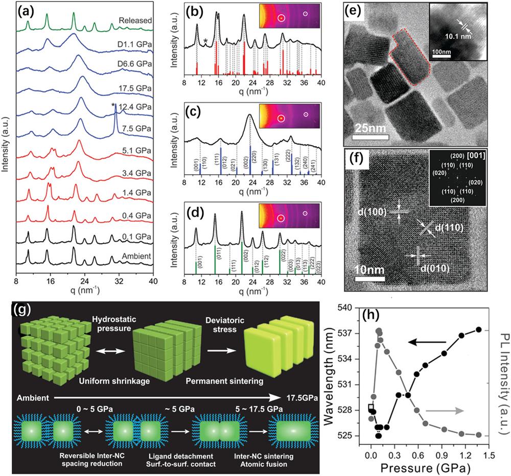
Nagaoka et al. investigated the pressure-induced behavior of CsPbBr3 nanocube superlattices (NC-SLs).98 Upon pressurization, individual CsPbBr3 NCs were fused into 2D nanoplatelets (NPLs). Figure 6(a) shows a sequence of wide-angle x-ray scattering (WAXS) patterns collected for NC-SLs from ambient pressure to 17.5 GPa, where multiple phase transitions were observed. The CsPbBr3 NCs were originally a mix of cubic and orthorhombic phases which transformed into a pure orthorhombic phase at 0.4 GPa [Fig. 6(b)]. The orthorhombic phase remained stable at 5.1 GPa. As pressure further increased, the three adjacent peaks of the orthorhombic phase [i.e., (112), (020), and (200)] combined to a single but broad peak, representing the amorphous-like phase which remained stable at 17.5 GPa [Fig. 6(c)]. The pressure-induced quasi-amorphous phase is an intermediate stage, revealing a short-range tetragonal ordering phase, as shown in Fig. 6(c). Upon decompression, the quasi-amorphous phase transformed into a cubic phase close to ambient pressure [Fig. 6(d)]. Thus, the direct crystallization of HP from amorphous precursors can result in the nucleation and growth of cubic HPV. In addition, the authors demonstrated the formation and preservation of pressure-driven NC-SLs by electron microscopy. Transmission electron microscopy (TEM) of the standing layered NPLs show they have a uniform thickness of 10 nm, which corresponds to 17 atomic layers [Fig. 6(e)]. The TEM image of the decompressed sample confirms the formation of a 2D single-crystal NPL with an edge length of 20–100 nm. The high-resolution (HR) TEM image [Fig. 6(f)] and the Fourier transform (FFT) pattern [Fig. 6(f), inset] show a single crystal cubic lattice, consistent with the WAXS results [Fig. 6(d)]. Using small-angle x-ray scattering analysis (SAXS), WAXS, and TEM, the authors proposed pressure-induced nucleation and growth of the 2D HPV NPLs [Fig. 6(g)]. Below 5.1 GPa, the SLs are in a hydrostatic state in which they maintain isotropy. When NC-SLs are compressed above 5.1 GPa, an anisotropic pressure gradient occurs on the SLs, causing deformation of the organic ligand; further increasing pressure leads to separation of the ligand from the NCs. After the separated ligands completely migrate out of the gap between the NCs, the NCs come in direct contact, facet-to-facet, and eventually fuse into 2D NPLs. Moreover, it is more noticeable that the PL peak of the CsPbBr3 NC-SLs shifted from 528 nm to 525 nm at 0.1 GPa, and the PL intensity was increased by about six times [Fig. 6(h)]. The authors suggest that the dramatic enhancement of emission may be caused by the reconstructed NC surfaces. When the pressure is totally released, a strong green emission reappears at 518 nm, whose intensity is 1.6 times higher than that of the initial emission.

Fig. 6. (a) WAXS patterns of CsPbBr3 nanocubes during compression and decompression. (b)–(d) Integrated WAXS spectra with calculated Bragg reflection positions at 1.4 GPa, 14.5 GPa, and total release of pressure, respectively. The bars represent the calculated Bragg reflection positions. (e) TEM image of the pressure-sintered NPLs. Inset shows the high-resolution (HR) TEM image of the pressurized sample with a lamellar structure before disassembly. (f) An HRTEM image and the corresponding FFT pattern (inset) of the pressure-synthesized CsPbBr3 NPLs. (g) Schematic demonstration of the pressure-sintering process: NC-SL evolution (top) and interparticle fusion (bottom). (h) Plots of the PL peak position of the NC-SL PLs (black) and the relative PL intensity (gray) as a function of pressure. The open square shows the PL intensity after decompression. These figures are reproduced with permission from Nagaoka et al., Adv. Mater. 29, 1606666 (2017). Copyright 2017 Wiley-VCH Verlag GmbH & Co. KGaA.98

下载图片 查看所有图片

Xiao et al. studied the pressure response of CsPbBr3 with various morphologies (nanocrystals, nanowires, and bulk materials), where simultaneous carrier lifetime prolongation and bandgap narrowing were observed.43 Morphology-dependent transition dynamics under high pressures were observed. The phase change interval of 0.58 GPa, ranging from 1.22 GPa to 1.80 GPa, of the nanowires is greater than that of the nanocrystals (0.26 GPa) but smaller than that of the bulk material (0.82 GPa). The bandgap redshift of 0.05 eV of CsPbBr3 nanowires is smaller than that of nanocrystals (0.11 eV) but larger than that of their bulk counterparts (0.02 eV). In comparison with bulk CsPbBr3, the pressure-dependent PL spectra of the nanowires experienced a similar process. The unique geometrical morphology effects were responsible for the different values of the phase change interval and the bandgap redshift among different CsPbBr3 materials.

2.5 C. Low-dimensional HPVs

Low-dimensional HPVs, possessing intrinsic quantum confinement effects, are promising for advanced photovoltaic and optoelectronic applications, especially for 2D layered compounds.101–107 In the 1990s, Mitzi et al. first synthesized a series of 2D organic–inorganic HPVs.108 In 2014, Dohner et al. reported corrugated-2D structures which exhibit white-light broadband emission.109 Large structure distortion and strong exciton-lattice coupling with efficient exciton self-trapping have been discovered in this kind of material. More recently, by further lowering the dimensionality of HPVs to one-dimension (1D), at the molecular level, stronger quantum confinement and exciton-lattice interaction were revealed, exhibiting broader emission.110 Furthermore, zero-dimensional (0D) compounds can be obtained by controlling the synthetic conditions where the octahedra or their clusters are completely isolated by organic molecules.80 Compared with their 3D counterparts, low-dimensional perovskites show enhanced stability, stronger quantum-confinement properties, and wider tunability.111–114 The PL of 3D MAPbX3 quenches rapidly and disappears at 2–3 GPa, making the tunability of emission energy (or color) very limited (usually less than 80 meV).15,47 Although the tunability of FAPbX3 is 40 meV larger,56,88,115 this level of tunability is still not good enough to optimize optoelectronic properties. The rapid quenching of PL can be attributed to the bending of chemical bonds and lattice distortion in the 3D structure.26,107 Due to the unique multiple quantum well structures which possess out-of-plane quantum and dielectric confinements, the class of 2D HPVs is emerging as a novel platform for high-pressure research.116 Recently, an increasing amount of high-pressure research has been reported on 2D HPVs.73,81,102,111

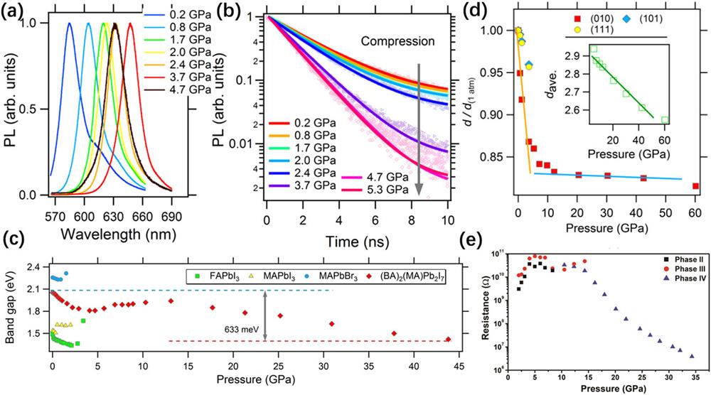
Liu et al. reported bandgap narrowing (633 meV) in an RP-type perovskite (BA)2(MA)Pb2I7 under pressure.112 The in situ high-pressure PL shows an apparent redshift of the PL peak position, from 587 nm at 1 atm to 648 nm at 3.7 GPa, and then a blueshift to 631 nm at 4.7 GPa [Fig. 7(a)]. As shown in the time-resolved PL spectra in [Fig. 7(b)], the lifetime increases monotonically with increasing pressure to 5.3 GPa. Generally, 3D HPVs exhibit a blue jump after a redshift in the lower pressure range (0.4 GPa for MAPbI3 and 2.0 GPa for FAPbI3) due to lattice distortion. It is worth noting that a second discontinuity was discovered at 13 GPa for 2D (BA)2(MA)Pb2I7, which is unobserved in 3D HPVs. Such a discontinuity triggers a further redshift at higher pressures, resulting in the bandgap narrowing to 633 meV [Fig. 7(c)]. A clear anisotropic compression has been demonstrated [Fig. 7(d)]. At 12.2 GPa, the volume collapse was generally attributed to b-axis shortening caused by the decreased d-spacing for the (040) reflection where the large organic cations permitting the large interlayer spaces. However, the b-axis was compressed by only 0.9% from 12.2 GPa to 42.5 GPa, much smaller than the average value of 8.1%. Wang et al. reported that the bandgap of 2D HPVs (C4H9NH3)2PbI4 decreases to below 1 eV at 35.0 GPa, and the carrier lifetime at 9.9 GPa is 20 times larger than that at ambient pressure.113 The electrical resistance dropped by four orders of magnitude at 34.0 GPa [Fig. 7(e)].

Fig. 7. (a) and (b) In situ static PL and time-resolved PL spectra of (BA)2(MA)Pb2I7 under high pressure. (c) Pressure-induced evolution of bandgap of (BA)2(MA)Pb2I7 and three 3D HPVs. (d) Pressure dependence of the relative changes in the d-spacing. These figures are reproduced with permission from Liu et al., ACS Energy Lett. 2, 2518–2524 (2017). Copyright 2017 American Chemical Society.112 (e) Pressure-induced evolution of the electrical resistance of (C4H9NH3)2PbI4. This figure is taken from Ref. 113.

下载图片 查看所有图片

Yin et al. focused on the optical properties of mechanically exfoliated nm-thin flakes of 2D perovskite (C4H9NH3)2PbI4.81 Obvious changes in the excitonic emissions from PL spectra were observed. By combining the optical results with in situ XRD results, a relationship between structural modifications in the inorganic [PbI4]2− layer and the excitonic properties was revealed. The presence of the orthorhombic P21/a phase at above 1.4 GPa decreases the Pb–I bond length and increases the Pb–I–Pb bond angle, resulting in a redshift of the excitonic bandgap. A bandgap narrowing of about 0.35 eV is achieved at 5.3 GPa before amorphization. In addition, phase transitions prolongate the carrier lifetime from 150 ps at the initial phase to 190 ps under mild pressure—along with enhanced PL, which stems from the pressure-induced strong radiative recombination of the trapped excitons. At higher pressures, the carrier lifetime decreases to 53 ps along with a decrease in PL emission, which is probably due to pressure-induced lattice distortion and amorphization. Therefore, 2D HPVs have shown great tunability in bandgap structures under high pressure, providing a new platform to realize desired structures and optical properties for potential technological applications.

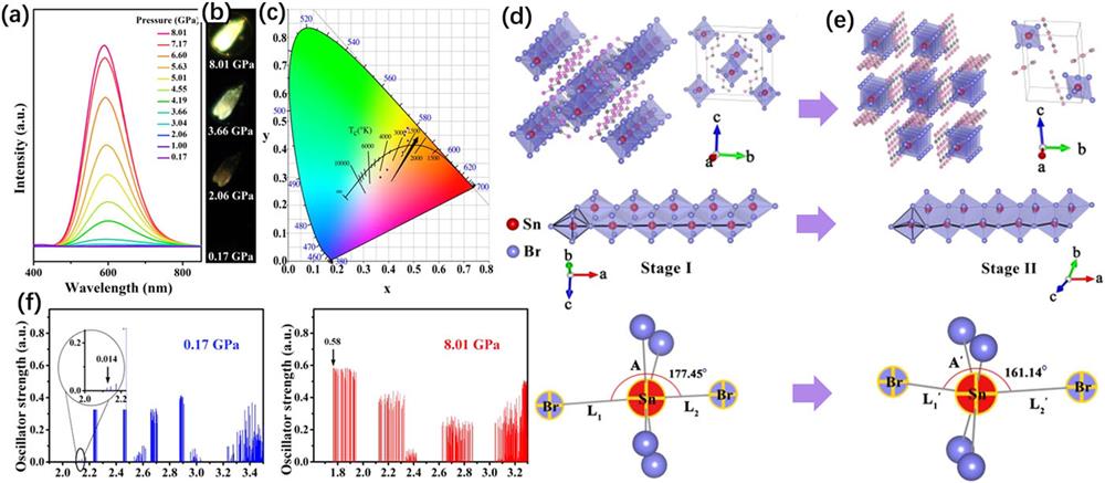
C4N2H14SnBr4 is a typical 1D HPV, in which the edge-sharing octahedral [SnBr4]2− anions are embraced by the organic [C4N2H14]2+ cations, serving as an assembly of core-shell quantum wires. Shi et al. reported an emergent emission of C4N2H14SnBr4 at pressures over ∼2 GPa.85 The PL intensity exhibits a continuous increase during compression until reaching the maximum value at 8 GPa [Fig. 8(a)]. Furthermore, the emission color changes from dark yellow to bright yellow under pressure [Fig. 8(b)] Pressure-dependent chromaticity coordinates of emission with increasing pressure from 2 GPa to 8 GPa are shown in Fig. 8(c). The authors claimed that C4N2H14SnBr4 undergoes a structural transformation from monoclinic I2/m to triclinic P1¯. Figures 8(d) and 8(e) show crystal structures of C4N2H14SnBr4 before and after the pressure-induced phase transition, and the corresponding Br–Sn–Br bond angle. First-principles calculations indicate that the pressure-induced emission is likely due to the enhanced transition dipole moment and the increased binding energy of self-trapped excitons (STEs) under high pressure [Fig. 8(f)].

Fig. 8. (a) Pressure-dependent PL spectra of 1D C4N2H14SnBr4. (b) PL images of C4N2H14SnBr4 under different pressures. (c) Pressure-dependent chromaticity coordinates. (d) and (e) Crystal structures and Br–Sn–Br bond length and angle of C4N2H14SnBr4 before and after the structural transition. (f) Calculation of the absorption oscillator strengths using the excited-state structure associated with STEs at 0.17 and 8.01 GPa. These figures are reproduced with permission from Shi et al., J. Am. Chem. Soc. 141, 6504–6508 (2019). Copyright 2019 American Chemical Society.85

下载图片 查看所有图片

In addition, Ma et al. reported that nonfluorescent 0D inorganic HPV Cs4PbBr6 nanocrystals exhibit strong emission under high pressure.11 PL appears at 3 GPa, the intensity increases with further compression and reaches a maximum at 6.2 GPa. The authors attributed the pressure-induced emission to the radiative recombination of the STEs associated with the large distortion of [PbBr6]4− octahedra after a phase transition. These high-pressure studies on low-dimensional HPVs demonstrate that pressure can not only be an effective tuner that modifies their optical properties, but also provides insights into understanding the relationship between structure and properties.

2.6 D. Other novel HPVs

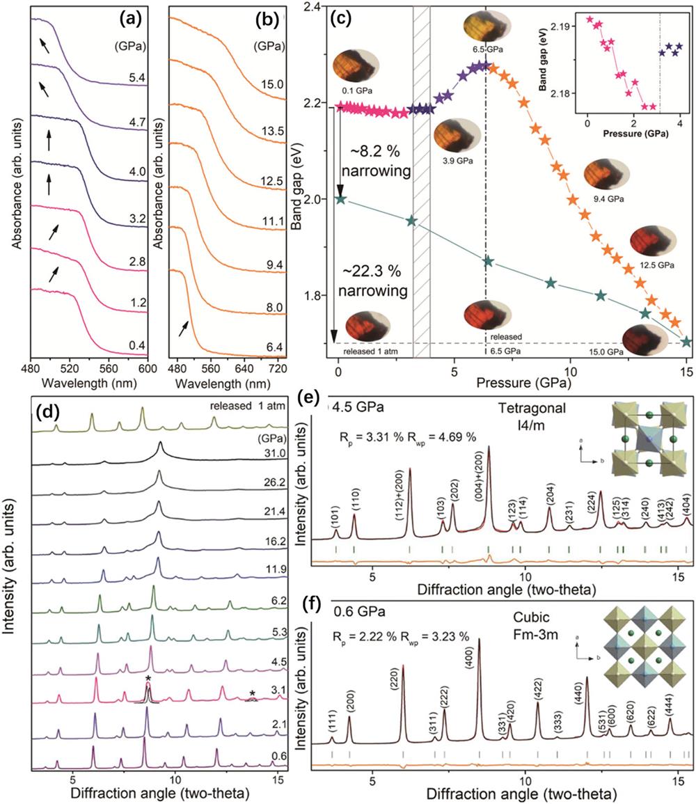
The halide-perovskite community continues to search for nontoxic, stable, and high-performance perovskite-like derivatives for photovoltaic and optoelectronic applications. Volonakis et al. reported the computational design and experimental synthesis of a new family of Pb-free inorganic halide double perovskites, such as Cs2BiAgCl6, materials that exhibit very promising optoelectronic properties, including tunable bandgaps in the visible range and low carrier effective masses.24 Li et al. reported a significant narrowing bandgap in this inorganic double perovskite by high-pressure treatment, from ∼2.2 eV at ambient pressure to 1.7 eV at 15 GPa [Figs. 9(a)–9(c)].83 Interestingly, the narrowed bandgap of Cs2AgBiBr6 can be partially retained after releasing pressure to ambient conditions due to incomplete recrystallization. Pressure-induced bandgap evolution is correlated with structural evolution. High-pressure Raman spectroscopy and angle-dispersive synchrotron XRD demonstrate that the Cs2AgBiBr6 transforms from the ambient cubic Pm3¯m phase to the tetragonal I4/m phase at 4.5 GPa [Figs. 9(d)–9(f)]. As unit cell contraction increases, broadening and weakened diffraction peaks indicate gradual structural amorphization [Fig. 9(d)].

Fig. 9. (a) and (b) UV-Vis absorption spectra of Cs2AgBiBr6 under high pressure. (c) Pressure-induced bandgap evolution of Cs2AgBiBr6, and representative optical micrographs. (d) Angle-dispersive synchrotron XRD patterns of Cs2AgBiBr6 at selected pressures. (e) and (f) Rietveld refinements of angle-dispersive synchrotron XRD patterns recorded at 0.6 and 4.5 GPa, respectively. These figures are reproduced with permission from Li et al., Angew. Chem., Int. Ed. 56, 15969–15973 (2017). Copyright 2017 Wiley-VCH Verlag GmbH & Co. KGaA.83

下载图片 查看所有图片

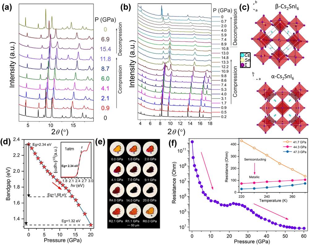
Bounos et al. investigated the pressure-induced evolution of the structures and properties of defective perovskite Cs2SnX6 (X = Cl, Br, and I).117 Upon compression, Cs2SnCl6 and Cs2SnBr6 maintain a face-centered cubic (fcc) structure up to 20 GPa [Fig. 10(a)], while Cs2SnI6 transforms initially from a cubic Pm3¯m phase to a more disordered structure at ∼3.3 GPa, and then to a low-symmetry monoclinic with an I2/m space group at about 8–10 GPa [Fig. 10(b)], which involves tilting and elongation of [SnI6]4− octahedra [Fig. 10(c)]. The structural changes of Cs2SnI6 are reversible upon pressure release. Wu et al. reported pressure-induced bandgap closure and metallization in perovskite analog Cs3Sb2I9.118 Cs3Sb2I9, with an initial bandgap of 2.34 eV reaching the Shockley–Queisser limit of 1.34 eV at 20.0 GPa [Fig. 10(d)], accompanied by obvious piezochromism from orange-yellow to opaque black [Fig. 10(e)]. These pressure-induced changes of the optical properties can be ascribed to atomic orbital overlap enhancement due to Sb–I bond-length contraction and Sb–I bond-angle diminution. Interestingly, Cs3Sb2I9 undergoes a semiconductor-to-metal transition during compression and shows metallic conduction at 44.3 GPa [Fig. 10(f)].

Fig. 10. High-pressure XRD patterns of (a) Cs2SnBr6 and (b) Cs2SnI6. (c) Two different crystal structures of Cs2SnI6, where the ambient pressure α-phase can be described as a body-centered tetragonal (BCT) unit cell with a lattice constant ratio c/a=2, while the high-pressure β-phase (I2/m) can be derived from the ambient BCT structure through the tilting of the SnI6 octahedra along the b axis. These figures are reproduced with permission from Bounos et al., J. Phys. Chem. C 122, 24004–24013 (2018). Copyright 2018 American Chemical Society.117 (d) Bandgap evolution of Cs3Sb2I9 at various pressures. The inset shows the bandgap Tauc plot of Cs3Sb2I9 at 1 atm. (e) Optical micrographs of Cs3Sb2I9 during compression. (f) The electrical resistance of Cs3Sb2I9 under high pressure. The inset shows the resistance-temperature diagram at different pressures. At 44.3 GPa, the electrical resistance of Cs3Sb2I9 increases with temperature ramping, suggesting the metallic behavior. These figures are reproduced with permission from Wu et al., ChemSusChem 12, 3971–3976 (2019). Copyright 2019 Wiley-VCH Verlag GmbH & Co. KGaA.118

下载图片 查看所有图片

The structural manipulation and property enhancements achieved by high-pressure treatment provide motivation for the further exploration and modification of the optoelectronic properties of HPVs, with various compositions, dimensionalities, and morphologies. By integrating high-pressure techniques and in situ characterization methods, one can systematically investigate the pressure-induced variation of structures and properties. Furthermore, the conclusions obtained from high-pressure research offer a new perspective for a fundamental understanding of the relationships among the different compositions, structures, dimensionalities, morphologies, and optoelectronic properties of HPVs, providing the potential for optimization of these materials for future photovoltaics and optoelectronics.

3 III. SUMMARY AND OUTLOOK

HPVs have been extensively investigated for their unique properties and potential applications in photovoltaic and optoelectronic devices. Perovskite derivatives, with various compositions, dimensionalities, and morphologies, have been developed, which show superior properties, such as better stability and wider tunability. Impressive progress has recently been made in high-pressure research concerning this family of materials. In this paper, we have summarized this progress, where the pressure-induced variations of structural, optical, electrical, and optoelectronic properties are discussed. We pay particular attention to the enhanced and emergent properties induced by pressure and the structure-property relationship. Despite these achievements, high-pressure research on HPVs still faces a number of challenges: (1) A solid understanding of HPVs is still far from satisfactory, which is partly the result of limited in situ characterization methods, especially for real devices; (2) The small samples used (usually at the microscale) can introduce issues of nonuniformity and increased complexity, increasing uncertainty; (3) The intrinsic sensitivity of HPVs to light and moist air cause irreversible degradation and introduce difficulties in obtaining accurate data.

Future high-pressure research on HPVs should include: (1) Achieving a deeper understanding of the structure-property relationship in a more comprehensive manner with the help of more systematic characterizations. For example, revealing the nature of pressure-induced amorphous or disordered structures is particularly interesting for understanding emergent properties at high pressure. To this end, pair distribution function analyses of synchrotron x-ray and neutron total scattering data can be used to explore the characteristics of local structures. (2) Alternative routes can be explored to simulate the high-pressure effects of DACs to realize unique structures and properties, e.g., by using a large-volume press, chemical tailoring, and interfacial engineering. (3) Developing theoretical simulations based on experimental results will provide mechanistic explanations and thus further our fundamental understanding.

References

[1] , et al.. Enhanced stability of perovskite solar cells using organosilane-treated double polymer passivation layers. J. Koraen Phys. Soc., 2018, 73: 1787-1793.

[2] , et al.. Organometal halide perovskites as visible-light sensitizers for photovoltaic cells. J. Am. Chem. Soc., 2009, 131: 6050-6051.

[3] , et al.. Highly efficient monolithic perovskite silicon tandem solar cells: Analyzing the influence of current mismatch on device performance. Sustainable Energy Fuels, 2019, 3: 1995-2005.

[4] , et al.. Improving charge transport via intermediate-controlled crystal growth in 2D perovskite solar cells. Adv. Funct. Mater., 2019, 29: 1901652.

[5] , et al.. Tunable polaron distortions control the extent of halide demixing in lead halide perovskites. J. Phys. Chem. Lett., 2018, 9: 3998-4005.

[6] , et al.. Facile method for the controllable synthesis of CsxPbyBrz-based perovskites. Inorg. Chem., 2018, 57: 6206-6209.

[7] , et al.. Perovskite LEDs. Sci. Video Protocols, 2019, 1: 1-5.

[8] , et al.. High color rendering index white-light emission from UV-driven LEDs based on single luminescent materials: Two-dimensional perovskites (C6H5C2H4NH3)2PbBrxCl4-x. ACS Appl. Mater. Interfaces, 2018, 10: 15980-15987.

[9] , et al.. Advances in perovskite solar cells. Adv. Sci., 2016, 3: 1500324.

[10] . Toward lead-free perovskite solar cells. ACS Energy Lett., 2016, 1: 1233-1240.

[11] , et al.. Pressure-induced emission of cesium lead halide perovskite nanocrystals. Nat. Commun., 2018, 9: 4506.

[12] , et al.. Two regimes of carrier diffusion in vapor-deposited lead-halide perovskites. J. Phys. Chem. C, 2017, 121: 21600-21609.

[13] . Chlorine doping reduces electron-hole recombination in lead iodide perovskites: Time-domain ab initio analysis. J. Phys. Chem. Lett., 2015, 6: 4463-4469.

[14] , et al.. Factors influencing the mechanical properties of formamidinium lead halides and related hybrid perovskites. ChemSusChem, 2017, 10: 3740-3745.

[15] . Organic-inorganic hybrid lead halide perovskites for optoelectronic and electronic applications. Chem. Soc. Rev., 2016, 45: 655-689.

[16] , et al.. Dynamic electronic junctions in organic–inorganic hybrid perovskites. Nano Lett., 2017, 17: 4831-4839.

[17] . What defines a perovskite?. Adv. Energy Mater., 2018, 8: 1802366.

[18] . Electro-optic response in germanium halide perovskites. J. Phys. Chem. Lett., 2018, 9: 1018-1027.

[19] . Review of recent progress in chemical stability of perovskite solar cells. J. Mater. Chem. A, 2015, 3: 8970-8980.

[20] , et al.. Effect of mechanical forces on thermal stability reinforcement for lead based perovskite materials. J. Mater. Chem. A, 2019, 7: 540-548.

[21] . Perovskites for photovoltaics: A combined review of organic-inorganic halide perovskites and ferroelectric oxide perovskites. J. Mater. Chem. A, 2015, 3: 18809-18828.

[22] , et al.. Pressure-tailored band gap engineering and structure evolution of cubic cesium lead iodide perovskite nanocrystals. J. Phys. Chem. C, 2018, 122: 9332-9338.

[23] , et al.. Organic-inorganic hybrid gold halide perovskites: Structural diversity through cation size. Chem. Eur. J., 2019, 25: 9885-9891.

[24] , et al.. Lead-free halide double perovskites via heterovalent substitution of noble metals. J. Phys. Chem. Lett., 2016, 7: 1254-1259.

[25] , et al.. Fashioning fluorous organic spacers for tunable and stable layered hybrid perovskites. Chem. Mater., 2018, 30: 8211-8220.

[26] , et al.. Low-dimensional organometal halide perovskites. ACS Energy Lett., 2017, 3: 54-62.

[27] . Halide perovskites under pressure: Accessing new properties through lattice compression. ACS Energy Lett., 2017, 2: 1549-1555.

[28] , et al.. Halide perovskite materials for solar cells: A theoretical review. J. Mater. Chem. A, 2015, 3: 8926-8942.

[29] , et al.. Pressures tuning the band gap of organic–inorganic trihalide perovskites (MAPbBr3): A first-principles study. J. Electron. Mater., 2018, 47: 7204-7211.

[30] , et al.. Organic cations might not be essential to the remarkable properties of band edge carriers in lead halide perovskites. Adv. Mater., 2017, 29: 1603072.

[31] , et al.. Electron–rotor interaction in organic–inorganic lead iodide perovskites discovered by isotope effects. J. Phys. Chem. Lett., 2016, 7: 2879-2887.

[32] , et al.. Pressure-induced dramatic changes in organic-inorganic halide perovskites. Chem. Sci., 2017, 8: 6764-6776.

[33] , et al.. Trap states in lead iodide perovskites. J. Am. Chem. Soc., 2015, 137: 2089-2096.

[34] , et al.. Between the sheets: Postsynthetic transformations in hybrid perovskites. Chem. Mater., 2017, 29: 1868-1884.

[35] , et al.. Excitonic states of alkylammonium lead-iodide layered perovskite semiconductors under hydrostatic pressure to 25 GPa. Phys. Status Solidi B, 2001, 223: 177-182.

[36] , et al.. CsSnI3: Semiconductor or metal? High electrical conductivity and strong near-infrared photoluminescence from a single material. High hole mobility and phase-transitions. J. Am. Chem. Soc., 2012, 134: 8579-8587.

[37] , et al.. Enhanced structural stability and photo responsiveness of CH3NH3SnI3 perovskite via pressure-induced amorphization and recrystallization. Adv. Mater., 2016, 28: 8663-8668.

[38] . Pressure-induced topological nontrivial phase and tunable optical properties in all-inorganic halide perovskites. J. Phys. Chem. C, 2018, 122: 17718-17725.

[39] , et al.. Low dimensional metal halide perovskites and hybrids. Mater. Sci. Eng., 2019, 137: 38-65.

[40] , et al.. Materials discovery at high pressures. Nat. Rev. Mater., 2017, 2: 17005.

[41] . Recent progress on high-pressure and high-temperature studies of fullerenes and related materials. Matter Radiat. Extremes, 2019, 4: 028201.

[42] , et al.. Recent advances in high-pressure science and technology. Matter Radiat. Extremes, 2016, 1: 59-75.

[43] , et al.. Pressure effects on structure and optical properties in cesium lead bromide perovskite nanocrystals. J. Am. Chem. Soc., 2017, 139: 10087-10094.

[44] . Criticality of symmetry in rational design of chalcogenide perovskites. J. Phys. Chem. Lett., 2018, 9: 248-257.

[45] . Chemistry at high pressure: Tuning functional materials properties. MRS Bull., 2017, 42: 718-723.

[46] . Ultrahigh-pressure transitions in solid hydrogen. Rev. Mod. Phys., 1994, 66: 671-692.

[47] . Photovoltaic hybrid perovskites under pressure. J. Phys. Chem. Lett., 2017, 8: 2496-2506.

[48] . Pressure-induced effects in organic–inorganic hybrid perovskites. J. Phys. Chem. Lett., 2017, 8: 2613-2622.

[49] , et al.. Superconductivity at 250 K in lanthanum hydride under high pressures. Nature, 2019, 569: 528-531.

[50] , et al.. Hydrogen confined in a single wall carbon nanotube becomes a metallic and superconductive nanowire under high pressure. Nano Lett., 2019, 19: 2537-2542.

[51] , et al.. Structural stability and optical properties of two-dimensional perovskite-like CsPb2Br5 microplates in response to pressure. Nanoscale, 2019, 11: 820-825.

[52] , et al.. Pressure-induced structural transition and band gap evolution of double perovskite Cs2AgBiBr6 nanocrystals. Nanoscale, 2019, 11: 17004-17009.

[53] , et al.. Conventional superconductivity at 203 kelvin at high pressures in the sulfur hydride system. Nature, 2015, 525: 73-76.

[54] , et al.. Pressure-induced phase transformation, reversible amorphization, and anomalous visible light response in organolead bromide perovskite. J. Am. Chem. Soc., 2015, 137: 11144-11149.

[55] , et al.. Pressure-induced metallization of the halide perovskite (CH3NH3)PbI3. J. Am. Chem. Soc., 2017, 139: 4330-4333.

[56] , et al.. Pressure-induced polymorphic, optical, and electronic transitions of formamidinium lead iodide perovskite. J. Phys. Chem. Lett., 2017, 8: 2119.

[57] , et al.. High-pressure-induced comminution and recrystallization of CH3NH3PbBr3 nanocrystals as large thin nanoplates. Adv. Mater., 2018, 30: 1705017.

[58] , et al.. P-T phase relations of CH3NH3PbX3 (X = Cl, Br, I) crystals. J. Phys. Chem. Solids, 1992, 53: 277-281.

[59] , et al.. New-generation integrated devices based on dye-sensitized and perovskite solar cells. Enegy Environ. Sci., 2018, 11: 476-526.

[60] , et al.. High-efficiency humidity-stable planar perovskite solar cells based on atomic layer architecture. Enegy Environ. Sci., 2017, 10: 91-100.

[61] . Materials chemistry approaches to the control of the optical features of perovskite solar cells. J. Mater. Chem. A, 2017, 5: 20561-20578.

[62] , et al.. Towards stable and commercially available perovskite solar cells. Nat. Energy, 2016, 1: 16152.

[63] . Metal-halide perovskites for photovoltaic and light-emitting devices. Nat. Nanotechnol., 2015, 10: 391-402.

[64] , et al.. Capturing the sun: A review of the challenges and perspectives of perovskite solar cells. Adv. Energy Mater., 2017, 7: 1700264.

[65] . Low-dimensional perovskites: From synthesis to stability in perovskite solar cells. Adv. Energy Mater., 2018, 8: 1702073.

[66] , et al.. Pressure response of an organic-inorganic perovskite: Methylammonium lead bromide. Chem. Mater., 2007, 19: 2401-2405.

[67] , et al.. Synthesis and crystal chemistry of the hybrid perovskite (CH3NH3)PbI3 for solid-state sensitised solar cell applications. J. Mater. Chem. A, 2013, 1: 5628-5641.

[68] , et al.. Locking of methylammonium by pressure-enhanced H-bonding in (CH3NH3)PbBr3 hybrid perovskite. J. Phys. Chem. Lett., 2017, 121: 28125-28131.

[69] , et al.. High pressure induced in situ solid-state phase transformation of nonepitaxial grown metal@semiconductor nanocrystals. J. Phys. Chem. Lett., 2018, 9: 6544-6549.

[70] , et al.. Pressure dependence of mixed conduction and photo responsiveness in organolead tribromide perovskites. J. Phys. Chem. Lett., 2017, 8: 2944-2950.

[71] . Mechanism of pressure-induced phase transitions, amorphization, and absorption-edge shift in photovoltaic methylammonium lead iodide. J. Phys. Chem. Lett., 2016, 7: 3458-3466.

[72] , et al.. New metallic ordered phase of perovskite CsPbI3 under pressure. Adv. Sci., 2019, 6: 1900399.

[73] , et al.. Direct-indirect transition of pressurized 2D halide perovskite: Role of benzene ring stack ordering. J. Phys. Chem. Lett., 2019, 10: 5687-5693.

[74] , et al.. Emission enhancement and bandgap retention of a two-dimensional mixed cation lead halide perovskite under high pressure. J. Mater. Chem. A, 2019, 7: 6357-6362.

[75] , et al.. Optical behaviors of a micro-sized single crystal MAPbI3 plate under high pressure. J. Phys. Chem. C, 2019, 123: 30221-30227.

[76] , et al.. Pressure-induced broadband emission of 2D organic-inorganic hybrid perovskite (C6H5C2H4NH3)2PbBr4. Adv Sci, 2019, 6: 1801628.

[77] , et al.. Pressure engineering of photovoltaic perovskites. Mater. Today, 2019, 27: 91-106.

[78] , et al.. Metal halide perovskite nanostructures for optoelectronic applications and the study of physical properties. Nat. Rev. Mater., 2019, 4: 169-188.

[79] , et al.. Interconversion between free charges and bound excitons in 2D hybrid lead halide perovskites. J. Phys. Chem. Lett., 2017, 121: 26566-26574.

[80] , et al.. Organic–inorganic metal halide hybrids beyond perovskites. Mater. Res. Lett., 2018, 6: 552-569.

[81] , et al.. Pressure-engineered structural and optical properties of two-dimensional (C4H9NH3)2PbI4 perovskite exfoliated nm-thin flakes. J. Am. Chem. Soc., 2018, 141: 1235-1241.

[82] , et al.. Simultaneous band-gap narrowing and carrier-lifetime prolongation of organic-inorganic trihalide perovskites. Proc. Natl Acad. Sci., 2016, 113: 8910-8915.

[83] , et al.. High-pressure band-gap engineering in lead-free Cs2AgBiBr6 double perovskite. Angew. Chem., Int. Ed., 2017, 56: 15969-15973.

[84] . Pressure-induced structural and optical properties of inorganic halide perovskite CsPbBr3. J. Phys. Chem. Lett., 2017, 8: 3752-3758.

[85] , et al.. Pressure-induced emission (PIE) of one-dimensional organic tin bromide perovskites. J. Am. Chem. Soc., 2019, 141: 6504-6508.

[86] . Pressure-induced structural and optical properties of organometal halide perovskite-based formamidinium lead bromide. J. Phys. Chem. Lett., 2016, 7: 2556-2562.

[87] , et al.. Pressure-induced structural evolution and band gap shifts of organometal halide perovskite-based methylammonium lead chloride. J. Phys. Chem. Lett., 2016, 7: 5273-5279.

[88] , et al.. Pressure-induced phase transition and band gap engineering in propylammonium lead bromide perovskite. J. Phys. Chem. C, 2019, 123: 15204-15208.

[89] , et al.. Unusual pressure-induced electronic structure evolution in organometal halide perovskite predicted from first-principles. Org. Electron., 2019, 67: 89-94.

[90] , et al.. High-pressure behavior of methylammonium lead iodide (MAPbI3) hybrid perovskite. J. Appl. Phys., 2016, 119: 185901.

[91] , et al.. High-pressure single-crystal structures of 3D lead-halide hybrid perovskites and pressure effects on their electronic and optical properties. ACS Cent. Sci., 2016, 2: 201-209.

[92] , et al.. Variable temperature and high-pressure crystal chemistry of perovskite formamidinium lead iodide: A single crystal X-ray diffraction and computational study. Chem. Commun., 2017, 53: 7537-7540.

[93] , et al.. Pressure-induced phase transitions and templating effect in three-dimensional organic-inorganic hybrid perovskites. Phys. Rev. B, 2003, 68: 020103.

[94] , et al.. Pressure-induced structural evolution, optical and electronic transitions of nontoxic organometal halide perovskite-based methylammonium tin chloride. Appl. Phys. Lett., 2017, 111: 233901.

[95] , et al.. Pressure effects on the inductive loop, mixed conduction, and photoresponsivity in formamidinium lead bromide perovskite. Appl. Phys. Lett., 2018, 113: 262105.

[96] , et al.. Pressure-induced phase transformation of CsPbI3 by X-ray diffraction and Raman spectroscopy. Phase Transition, 2017, 91: 38-47.

[97] , et al.. Pressure-induced structural evolution and optical properties of metal-halide perovskite CsPbCl3. J. Phys. Chem. C, 2018, 122: 15220-15225.

[98] , et al.. Nanocube superlattices of cesium lead bromide perovskites and pressure-induced phase transformations at atomic and mesoscale levels. Adv. Mater., 2017, 29: 1606666.

[99] , et al.. Pressure response of photoluminescence in cesium lead iodide perovskite nanocrystals. J. Phys. Chem. C, 2018, 122: 11024-11030.

[100] , et al.. Tunable photoluminescence and an enhanced photoelectric response of Mn2+-doped CsPbCl3 perovskite nanocrystals via pressure-induced structure evolution. Nanoscale, 2019, 11: 11660-11670.

[101] , et al.. A zero-dimensional organic seesaw-shaped tin bromide with highly efficient strongly stokes-shifted deep-red emission. Angew. Chem., Int. Ed., 2018, 57: 1021-1024.

[102] , et al.. High pressure structural and optical properties of two-dimensional hybrid halide perovskite (CH3NH3)3Bi2Br9. Inorg. Chem., 2019, 58: 1621-1626.

[103] , et al.. Thousand-fold conductivity increase in 2D perovskites by polydiacetylene incorporation and doping. Angew. Chem., Int. Ed., 2018, 57: 13882-13886.

[104] , et al.. 2D homologous perovskites as light-absorbing materials for solar cell applications. J. Am. Chem. Soc., 2015, 137: 7843-7850.

[105] , et al.. Composition engineering in two-dimensional Pb-Sn-Alloyed perovskites for efficient and stable solar cells. ACS Appl. Mater. Interfaces, 2018, 10: 21343-21348.

[106] . Low-dimensional-networked metal halide perovskites: The next big thing. ACS Energy Lett., 2017, 2: 889-896.

[107] , et al.. Luminescent zero-dimensional organic metal halide hybrids with near-unity quantum efficiency. Chem. Sci., 2018, 9: 586-593.

[108] , et al.. Conducting layered organic-inorganic halides containing -oriented perovskite sheets. Science, 1995, 267: 1473-1476.

[109] . Self-assembly of broadband white-light emitters. J. Am. Chem. Soc., 2014, 136: 1718-1721.

[110] , et al.. One-dimensional organic lead halide perovskites with efficient bluish white-light emission. Nat. Commun., 2017, 8: 14051.

[111] , et al.. Manipulating efficient light emission in two-dimensional perovskite crystals by pressure-induced anisotropic deformation. Sci. Adv., 2019, 5: eaav9445.

[112] , et al.. Two regimes of bandgap red shift and partial ambient retention in pressure-treated two-dimensional perovskites. ACS Energy Lett., 2017, 2: 2518-2524.

[113] , et al.. Large band gap narrowing and prolonged carrier lifetime of (C4H9NH3)2PbI4 under high pressure. Adv. Sci., 2019, 6: 1900240.

[114] . Red-to-black piezochromism in a compressible Pb–I–SCN layered perovskite. Chem. Mater., 2016, 28: 3241-3244.

[115] , et al.. Pressure-induced fluorescence enhancement of FAαPbBr2+α composite perovskites. Nanoscale, 2019, 11: 5868-5873.

[116] , et al.. Efficient blue electroluminescence using quantum-confined two-dimensional perovskites. ACS Nano, 2016, 10: 9720-9729.

[117] , et al.. Defect perovskites under pressure: Structural evolution of Cs2SnX6 (X = Cl, Br, I). J. Phys. Chem. C, 2018, 122: 24004-24013.

[118] , et al.. High-pressure band-gap engineering and metallization in the perovskite derivative Cs3Sb2I9. ChemSusChem, 2019, 12: 3971-3976.

Mei Li, Tianbiao Liu, Yonggang Wang, Wenge Yang, Xujie Lü. Pressure responses of halide perovskites with various compositions, dimensionalities, and morphologies[J]. Matter and Radiation at Extremes, 2020, 5(1): 018201.
引用该论文: TXT   |   EndNote

相关论文

加载中...

关于本站 Cookie 的使用提示

中国光学期刊网使用基于 cookie 的技术来更好地为您提供各项服务,点击此处了解我们的隐私策略。 如您需继续使用本网站,请您授权我们使用本地 cookie 来保存部分信息。
全站搜索
您最值得信赖的光电行业旗舰网络服务平台!