光学学报, 2020, 40 (20): 2025001, 网络出版: 2020-09-19
多层PtSe2/TiO2纳米棒肖特基结紫外光电探测器  下载: 1138次
Multilayer PtSe2/TiO2 NRs Schottky Junction for UV Photodetector
图 & 表
图 1. 器件结构示意图及材料表征。(a)器件结构示意图,插图为PtSe2/TiO2表面的内建电场;(b) TiO2 NRs的表面SEM图,插图为放大图;(c) TiO2 NRs的侧面SEM图;(d) FTO和生长于FTO上的TiO2 NRs的XRD射图;(e) PtSe2薄膜的SEM图;(f) PtSe2薄膜的高度剖面图,插图为PtSe2薄膜的AFM图
Fig. 1. Diagram of device structure and material characterization. (a) Diagram of device structure, inset shows built-in electric field at PtSe2/TiO2 surface; (b) top view SEM image of TiO2 NRs, inset shows magnification of SEM image; (c) cross-sectional view SEM image of TiO2 NRs; (d) XRD pattern of FTO and TiO2 NRs grown on FTO; (e) SEM image of PtSe2 film; (f) height profile of PtSe2 film, inset shows AFM image of PtSe2
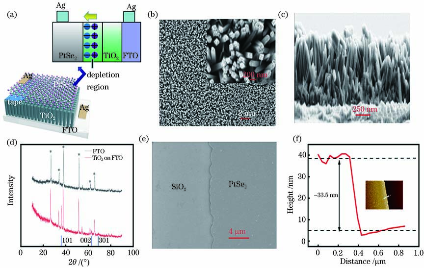
图 2. 二维材料PtSe2的结构和组成。(a) HRTEM图;(b)拉曼光谱;(c) Pt 4 f的XPS图;(d) Se 3 d的XPS图
Fig. 2. Structure and composition of two-dimensional material PtSe2. (a) HRTEM image; (b) Raman spectrum; (c) XPS image of Pt 4 f; (d) XPS image of Se 3 d

图 3. 器件对365 nm光的响应曲线及能带图。(a) I-V曲线,插图为在黑暗中暗电流取对数坐标的I-V特性;(b) -1.0 V偏压下365 nm光照下的光响应;(c)能带图;(d)器件在大约200个周期下的光响应;(e)空气环境中器件在5周之前和之后的光响应
Fig. 3. Response curves to 365 nm light and energy band diagram of proposed device. (a) I-V curve, inset shows I-V characteristic of dark current in logarithmic coordinates; (b) photo response under 365 nm light illumination at bias voltage of -1.0 V; (c) energy band diagram; (d) photo response of device for about two hundreds cycles of operation; (e) photo response of device before and after 5 weeks in air ambient condition

图 4. 不同光功率密度下的电学性能。(a) I-V曲线;(b)器件在-1.5 V偏压下的光响应;(c)光电流和光功率密度的拟合曲线;(d)在-1.5 V偏压下,Ilight/Idark与光功率密度的关系;(e)响应度和比探测率随入射光功率密度的变化;(f) -1.5 V偏压下,ηEQE与光功率密度的关系
Fig. 4. Electrical performance under different optical power densities. (a) I-V curve; (b) photo response of device at bias voltage of -1.5 V; (c) fitting curve of photocurrent and optical power density; (d) relationship between Ilight/Idark and optical power density at bias voltage of -1.5 V; (e) change of responsivity and specific detection rate with incident light power density; (f) relationship between ηEQE and optical power density at bia

图 5. 器件的光吸收和光响应。(a)器件的光谱响应;(b) TiO2、PtSe2和器件的吸收光谱;(c)在频率为1 Hz,365 nm光照下器件的响应曲线;(d)器件的上升和下降时间
Fig. 5. Light absorption and response of device. (a) Spectral response of device; (b) absorption spectra of TiO2, PtSe2, and device; (c) response curve of device under 365 nm irradiation with a frequency of 1 Hz; (d) rise time and fall time of device


表 1PtSe2/TiO2 NRs阵列光电探测器和其他基于TiO2的异质结器件的参数比较
Table1. Comparison of parameters of PtSe2/TiO2 NRs array photodetector and other TiO2-based heterojunction devices
|
陈红云, 鲁玉, 李辰, 赵兴远, 张秀星, 张致翔, 罗林保. 多层PtSe2/TiO2纳米棒肖特基结紫外光电探测器[J]. 光学学报, 2020, 40(20): 2025001. Hongyun Chen, Yu Lu, Chen Li, Xingyuan Zhao, Xiuxing Zhang, Zhixiang Zhang, Linbao Luo. Multilayer PtSe2/TiO2 NRs Schottky Junction for UV Photodetector[J]. Acta Optica Sinica, 2020, 40(20): 2025001.


 PDF全文
PDF全文

