Photonics Research, 2020, 8 (10): 10001634, Published Online: Sep. 29, 2020   

High-gain waveguide amplifiers in Si3N4 technology via double-layer monolithic integration Download: 592次

Author Affiliations
Optical Sciences Group, MESA+ Institute for Nanotechnology, University of Twente, 7500 AE Enschede, The Netherlands
Abstract
Silicon nitride (Si3N4)-on-SiO2 attracts increasing interest in integrated photonics owing to its low propagation loss and wide transparency window, extending from 400 nm to 2350 nm. Scalable integration of active devices such as amplifiers and lasers on the Si3N4 platform will enable applications requiring optical gain and a much-needed alternative to hybrid integration, which suffers from high cost and lack of high-volume manufacturability. We demonstrate a high-gain optical amplifier in Al2O3:Er3+ monolithically integrated on the Si3N4 platform using a double photonic layer approach. The device exhibits a net Si3N4-to-Si3N4 gain of 18.1±0.9 dB at 1532 nm, and a broadband gain operation over 70 nm covering wavelengths in the S-, C- and L-bands. This work shows that rare-earth-ion-doped materials and in particular, rare-earth-ion-doped Al2O3, can provide very high net amplification for the Si3N4 platform, paving the way to the development of different active devices monolithically integrated in this passive platform.

1. INTRODUCTION

Integrated waveguide amplifiers and light sources are essential components for photonic integrated circuits that combine different functionalities on a single chip [1]. Currently, silicon-on-insulator [2,3], indium phosphide [4,5], and silicon nitride (Si3N4) [6,7] are three commercially available photonic platforms. The Si3N4 platform, due to its low propagation loss (0.1  dB/cm) and wide transparency window (400  nm to 2.35 μm) [7], has achieved tremendous progress in passive applications including microwave photonics [8], nonlinear photonics [9], bio-sensing [10], quantum technology [11], and lidar [12]. The integration of active components such as amplifiers and lasers onto the passive Si3N4 platform will permit profiting from its excellent passive characteristics.

III-V semiconductor optical amplifiers have been hybrid integrated with the Si3N4 platform by butt-coupling to produce external cavity lasers [1315" target="_self" style="display: inline;">–15]. However, sophisticated assembly and packaging steps with high-precision alignment of the facets of the waveguides are required to achieve the high performance of such hybrid lasers [16], precluding cost-effective scaling of manufacturing, especially in the case of devices with complex optical functionalities and high integration density, where many transitions between the active and passive sections are required. Heterogeneous integration of III-V semiconductor optical amplifiers onto Si3N4 by micro-contact printing [17] has been proposed toward a more scalable solution.

Recently, monolithic integration of rare-earth-ion-doped (RE3+) aluminum oxide (Al2O3) and Si3N4 was demonstrated [1823" target="_self" style="display: inline;">23], showing potential for high-performance scalable light sources on the Si3N4 platform. Compared to III-V semiconductors [24], RE3+-ion-doped materials have a longer excited-state lifetime (0.1–10 ms) [25] and less refractive index change (106) [26] induced by the excitation of the doped ions, properties that are beneficial for thermally and spatially stable gain [27]. The high rare-earth ion dopant concentration achievable in crystalline host materials has allowed the demonstration of very high gain per unit length in an Yb3+-doped KY(WO4)2 waveguide (935  dB/cm at 980 nm) [28] and in an Er3+-doped chloride silicate nanowire (100  dB/cm at 1530 nm). However, such crystalline devices are difficult to fabricate [29] and to integrate onto a passive photonic platform for the development of more complex functionalities. Amorphous host materials can typically be deposited at the wafer level leading to simpler fabrication and integration schemes. Several host materials have been demonstrated, including Ta2O5 doped with both Er3+ and Yb3+ [30], TeO2 doped with Er3+ [31] and Tm3+ [32], and Al2O3 doped with Nd3+, Yb3+, Er3+, Tm3+, and Ho3+ [19,25,3335" target="_self" style="display: inline;">–35] to achieve emission at different wavelengths. Those materials are mainly deposited by reactive co-sputtering, although recent studies on rare-earth-ion-doped Al2O3 deposited by atomic layer deposition have shown very high gain per unit length (i.e., 20.1±7.31  dB/cm net modal gain in Al2O3:Er3+) [23] thanks to the control of Al2O3 and Er2O3 at the sub-atomic level. High-speed [27] and high internal net gain [36] optical amplifiers and narrow linewidth lasers [21,37] have also been demonstrated in Al2O3. Although both high net modal gain per unit length as well as high total net gain have been shown, high total gain (i.e., from Si3N4 to Si3N4) on a waveguide amplifier integrated onto a passive photonic platform has not yet been reported.

In this work, we present an integrated high total gain (i.e., from passive waveguide to passive waveguide) optical amplifier in Al2O3:Er3+ monolithically integrated onto the Si3N4 platform via a double-layer platform [38]. Different from previous integration methodologies in which the Al2O3:RE3+ material was directly deposited onto Si3N4 elements [20,21,23,31] or sputtered into SiO2 trenches within the Si3N4 platform [19,22], in our approach the Al2O3:RE3+ and the Si3N4 waveguides are located in two individual layers separated by a thin SiO2 film. The optical modes are therefore guided independently in each of the photonic layers permitting their independent optimization to minimize losses and to maximize the overlap between pump and signal modes on the active waveguides. The transfer of modes between the two layers is achieved via vertically tapered adiabatic couplers that exhibit low loss, broadband behavior, and high tolerance to overlay errors. Such tapers have already been demonstrated in our previous work [38,39]. A total gain as high as 18.1±0.9  dB was achieved at 1532 nm for amplifiers with a 10 cm long gain section with more than 70 nm bandwidth of net gain.

2. RESULTS

Figure 1(a) shows the schematic view of the monolithic Al2O3:Er3+-Si3N4 amplifier chip consisting of the Al2O3:Er3+, the Si3N4 waveguides, and the adiabatic couplers. Two hundred nanometer thick Si3N4 waveguides with a width of 1.4 μm are designed to be located on the bottom layer fabricated on silicon wafers with 8 μm thick thermal oxide as undercladding. This oxide thickness was found to be enough to prevent the mode from leaking into the Si substrate [38]. A 199.6±0.13  nm thick Si3N4 layer was deposited using low-pressure chemical vapor deposition (LPCVD). The Si3N4 waveguides were then patterned using i-line contact lithography followed by reactive ion etching (RIE) with CHF3 and O2 chemistry, which provides an etching rate of 30 nm/min for Si3N4 and 32 nm/min for SiO2. The fabricated waveguides have a width of WP=1.4±0.08  μm and a measured propagation loss of 0.14 dB/cm at the wavelength of 1532 nm, measured using reference add-drop ring resonators. Multi/demultiplexers for combining/splitting the pump and signal modes were integrated on the passive Si3N4 waveguides [40].
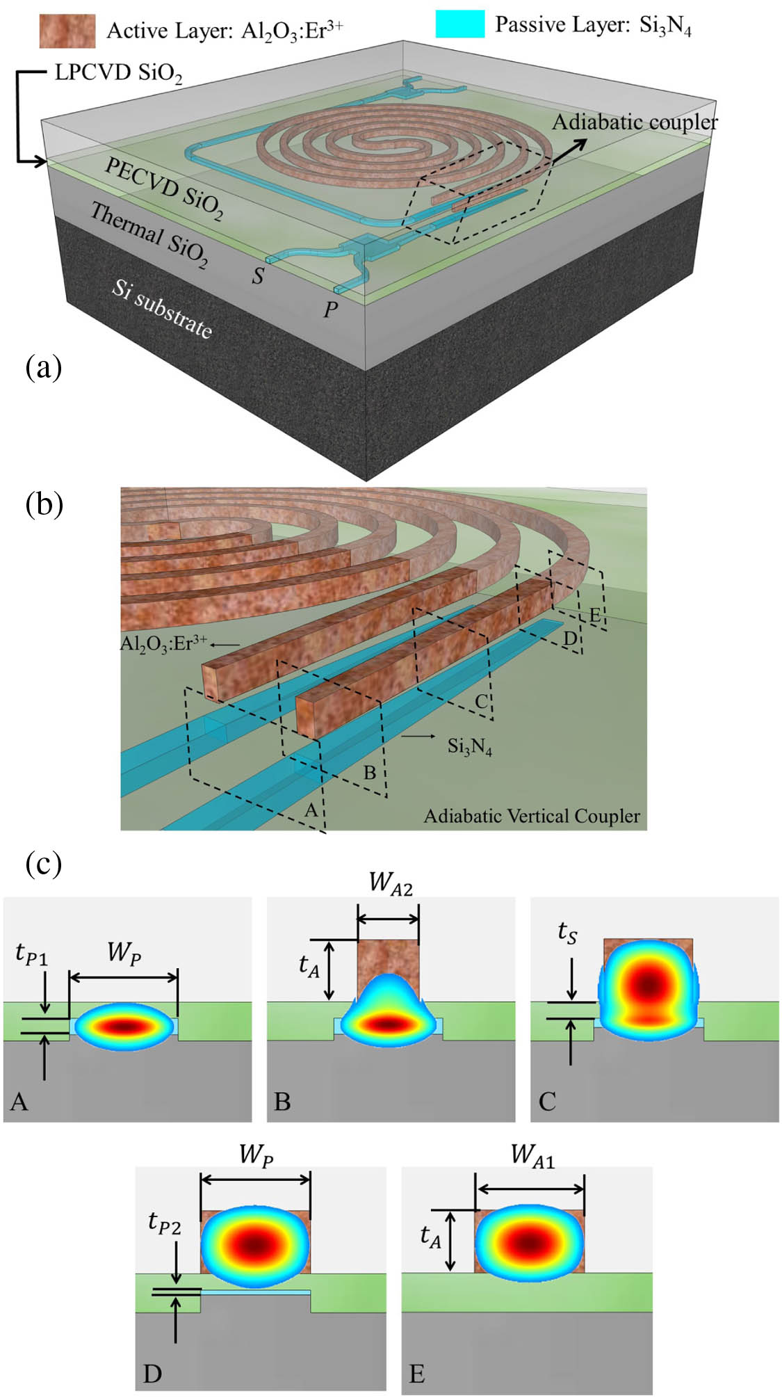
Fig. 1. Structure of the monolithically integrated Al2O3:Er3+-Si3N4 amplifier. (a) 3D schematic of the whole amplifier chip with MMI-based multi/demultiplexer. P and S indicate the pump port and the signal port of the MMI multi/demultiplexer, respectively. (b) Schematic of the adiabatic vertical coupler, consisting of a vertical Si3N4 taper and a lateral Al2O3:Er3+ taper. (c) Cross sections of the adiabatic coupler at different positions (A, B, C, D, E) indicated in (b) within the taper region along the propagation direction, and the related mode intensity profiles under transverse electric (TE) polarization. The different cross-sectional parameters are indicated. The field intensity is visualized in the rainbow color scale, where the highest intensity is represented by the red.

下载图片 查看所有图片

Between the Si3N4 and Al2O3:Er3+ layers, a TEOS SiO2 film was deposited as a spacer by LPCVD followed by an annealing step. The spacer provides not only a surface with good uniformity on top of which to deposit the Al2O3:Er3+ layer but also protects the top surface of the Si3N4 waveguides during the fabrication of the fully etched Al2O3:Er3+ waveguides. Simulations have shown that spacer thicknesses in the range 100–200 nm lead to both good optical coupling and good tolerance to the mask overlay errors [38] between the Si3N4 and Al2O3:Er3+ waveguides in the adiabatic coupler. To achieve this spacer thickness, a chemical mechanical polishing step was applied to reduce the thickness of the as-deposited LPCVD TEOS SiO2 layer from 760±6  nm to 180±16  nm [tS in Fig. 1(c)]. The Al2O3:Er3+ layer was then deposited by RF reactive co-sputtering with a target Er3+ concentration of 1.7×10²⁰  cm3. A layer thickness of tA=804±5  nm was measured at the location of the amplifier in the wafer. The Al2O3 waveguides were then patterned by i-line lithography and etched to a depth of 840 nm (overetching 36  nm into the SiO2 buffer layer) using RIE with a BCl3 and HBr chemistry.

Both the pump and the signal modes are transferred between the Al2O3:Er3+ and Si3N4 waveguides through adiabatic couplers, shown in Fig. 1(b). The couplers consist of a thickness-tapered Si3N4 waveguide and a width-tapered Al2O3:Er3+ waveguide [38,39]. The mode profile evolution along the adiabatic taper is illustrated in Fig. 1(c). The usage of waveguide tapers reduces the mode mismatch losses at the taper tips, namely the losses due to the overlap mismatch between the mode in A–B and D–E [Fig. 1(c)]. To achieve such high-performance coupling, the Al2O3:Er3+ waveguide was tapered laterally to a tip width of WA2=0.8±0.11  μm (i.e., limit of the UV contact lithography), while the Si3N4 waveguide was vertically tapered to a tip thickness of tP2=30.8±4  nm. The tapering was realized using the high-yield wet-etching process, which is the same as the one in Ref. [38]. A taper tip thickness below 50 nm is needed to achieve adiabatic condition and a tolerance of 0.6 μm to the mask overlay error between the Si3N4 and Al2O3 waveguides. The angle of the adiabatic taper originates from the etching speed difference between the Si3N4 and native SiO2 (sacrificial layer). Both tapers have the same length, 800 μm, resulting in an adiabatic angle of 0.007° for the lateral Al2O3:Er3+ taper and 0.013° for the vertical Si3N4 taper.

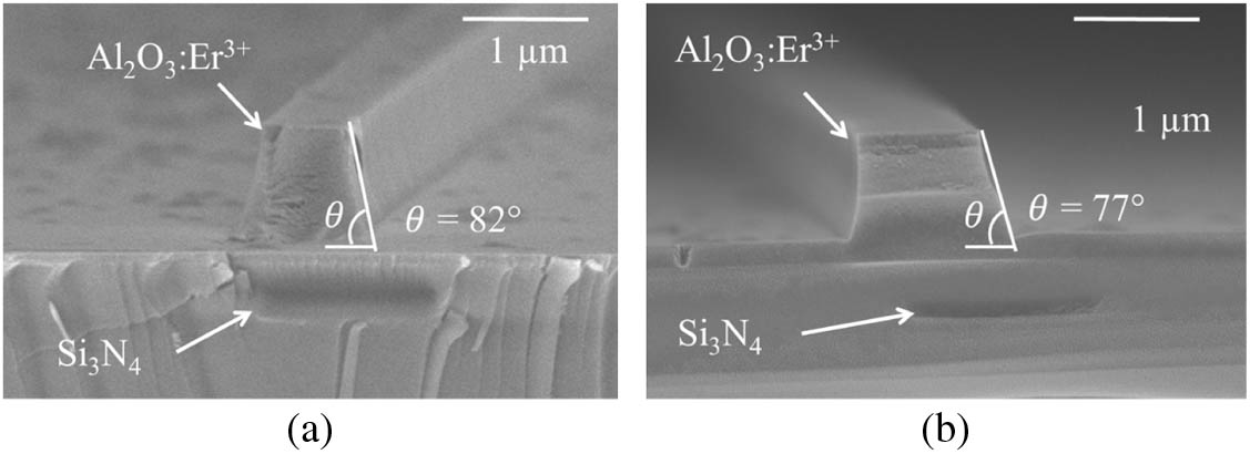
For the active Al2O3:Er3+ waveguide, monomode operation was chosen for both the pump (980 nm) and signal (C-band) wavelengths under transverse electric (TE) polarization. The overlap between the pump and signal modes was also maximized (88%) to achieve as high as possible optical gain. This value is higher than that under TM polarization. Furthermore, the on-chip multi/demultiplexers are also designed to operate under TE polarization. The total length of the spiral waveguide amplifier is designed to be 10 cm with a minimum radius of 250 μm, i.e., the radius of the S-bend in the center, at which the bend loss is less than 104  dB/cm and can be therefore neglected. The fully etched fabricated waveguides have a width of WA1=1.4±0.12  μm and a sidewall angle below 15° (Fig. 2).

Fig. 2. SEM images of the cross sections (a) nearby the tip of the Al2O3 taper and (b) nearby the tip of the Si3N4 taper. The SEM images were captured from a cleaved sample from a monitor wafer with undoped Al2O3 on the Si3N4 platform.

下载图片 查看所有图片

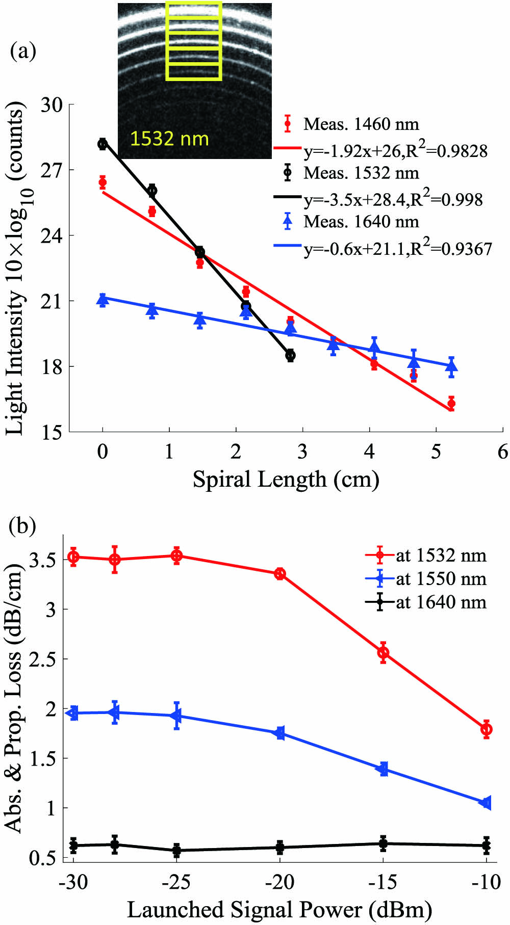
The loss from input to output of Si3N4 waveguide consists of the loss of the two Si3N4 to Al2O3 adiabatic couplers (αc) plus the total propagation loss of the spiral. The total loss per unit length of the Al2O3:Er3+ waveguides, αap, consists of (i) the propagation loss (αp), mainly caused by scattering due to the roughness of the sidewalls of the waveguide, which is assumed to be uniform along the length of the waveguide, and (ii) the absorption loss (αa), due to the absorption of the Er3+ ions excited from the ground state by the signal light. The absorption loss depends on the population of the ground state and, therefore, on the intensity of the signal used in the measurement. For the characterization of the gain of an amplifier using the signal enhancement method [23,36,41], the absorption loss in the small signal regime, i.e., for small enough signal so that the absorption cross section of the Er3+ ions is constant, should be used. In this work, a non-destructive method [36,42] based on the measurement of the scattered light from the top of the waveguide was employed to measure the αap of the spirals. Top-view intensity images of the scattered signal light propagating along the integrated Al2O3:Er3+ spiral amplifier, Fig. 3(a), were captured by an IR camera (InGaAs camera, Xenics Bocat 320). The intensity of the scattered light is proportional to the power of the mode traveling through the spiral [42], which follows a Lambert–Beer law [36] behavior along the propagation direction. Fitting an exponential decay to the measured intensity allows the determination of αap. The mode field diameter of the input fiber is considered as 10±0.5  μm and 6.6±0.5  μm for signal and pump wavelengths, respectively. The calculated fiber-to-chip coupling loss in the amplifier chip is 12 dB and 10 dB per facet for the wavelengths of 980 nm and 1550 nm, respectively, calculated by overlapping the waveguide mode with the fiber mode. It is important to highlight that this loss measurement method is independent of the fiber-to-chip coupling losses.

Fig. 3. Characterization of losses. (a) Measured intensity of the light scattered along the length of the Al2O3:Er3+ waveguide spirals at different wavelengths. Launched signal power is 30  dBm. (b) Measured absorption plus propagation losses of the Al2O3:Er3+ waveguide spiral as a function of launched signal power.

下载图片 查看所有图片

Figure 3(a) plots the binned counts originating from the yellow boxes shown in the inset of the figure, which are placed along the circular path of the spiral at the launched signal power of 30  dBm (i.e., measured incident power 20  dBm). From the least squares fitting of the data, absorption plus propagation losses (αap) of 1.92±0.10  dB/cm, 3.5±0.09  dB/cm, and 0.6±0.06  dB/cm at the wavelengths of 1460 nm, 1532 nm, and 1640 nm, respectively, were measured. The same characterization and fitting procedure were repeated for different launched signal powers to determine how small the launched signal power should be to satisfy small signal regime where the ground-state excitation reaches its maximum [Fig. 3(b)]. When the launched signal power is lower than 15  dBm, αap converges with less than 0.1 dB/cm variation.

Using the launched signal power of 30  dBm, αap was characterized in the full spectral window 1460–1640 nm, as shown in Fig. 4(a) (black triangles). αap values converge to a range of 0.6–0.7 dB/cm at a wavelength longer than 1610 nm, the wavelength range in which propagation loss dominates the αap. To verify the propagation losses, a similar measurement was carried out at a wavelength of 1306 nm (outside the ground-state absorption band of Er3+ ions) using the same spiral. A propagation loss of 0.64±0.05  dB/cm was measured, which is within the range of values measured at wavelengths longer than 1610 nm. Furthermore, using the absorption cross sections (σabs) for Er3+ in Al2O3 reported in previous work [41], we calculated the absorption spectrum by the following equation:

(a) Measured absorption plus propagation losses as a function wavelength for a launched signal power of 30  dBm. The red line shows the calculated values from the absorption cross sections presented in the work of Ref. [41] for an ion concentration of 1.65×10²⁰  cm3. (b) Transmitted power as a function of the number of Al2O3:Er3+-Si3N4 adiabatic couplers at the wavelength of 1306 nm. A loss per coupler of 0.49 dB was obtained. (c) Si3N4 multi/demultiplexer loss spectra by launching through the pump and signal ports at the wavelength of 1460–1635 nm. The shadows indicate the standard deviation of the measurement.

where N0 is the ion concentration in cm3 and Γ is the confinement factor of the mode inside the waveguide core. The calculated confinement factor at 1532 nm is 68.4% for the fabricated waveguide. The absorption curve takes into account the measured background propagation loss of the Al2O3:Er3+ waveguide of 0.64 dB/cm. It can be seen that the experimental data matches closely with the calculated absorption losses at the erbium concentration of 1.65×10²⁰  cm3, as shown in Fig. 4(a).

The Al2O3:Er3+-Si3N4 coupler loss (αc) was determined from the transmitted power of Si3N4 waveguides with different number of cascaded couplers fabricated in the same wafer as the spiral amplifiers. A mask overlay error below 0.4 μm was determined by means of reference Vernier rulers. The characterization was carried out at a wavelength of 1306 nm using the experimental setup described in our previous work [38,39], and it is plotted in Fig. 4(b). An average loss of 0.49±0.02  dB per coupler was measured. Similar losses at the wavelengths of 980 nm and 1550 nm are expected for the adiabatic coupler regardless of the absorption of Er3+ ions, by referring to the ultra-broadband performance of the adiabatic coupler shown in the previous work [39].

Furthermore, the insertion loss of the on-chip MMI multi/demultiplexer was experimentally characterized in the spectral window of 1460–1635 nm, as shown in Fig. 4(c). The characterization used the same experimental setup as the work of Ref. [40]. By launching the signal light through the signal (S) port and pump (P) port, the MMI losses were measured to be 1.38±0.1  dB and 9.03±0.04  dB at the wavelength of 1532 nm, respectively. At the pump wavelength, i.e., 976.2 nm, the MMI loss was 2.7±0.6  dB by launching the light through the pump port. In this work, we focus on the monolithic integrated amplifier. The optimization of the MMI multi/demultiplexer can be found in Ref. [40].

The net gain of the optical amplifiers (in decibels) from the input Si3N4 waveguide to the output Si3N4 waveguide was obtained using the following equation [23,36,42]: where the first term is known as signal enhancement, defined as the ratio of the output power of the signal with the pump on (Pons) corrected to eliminate the contribution of the amplified spontaneous emission (ASE) and the output power with the pump off (Poffs); the second term represents the total absorption and propagation losses of a spiral of length L; and the last term represents the losses introduced by the two Si3N4Al2O3 adiabatic couplers. During gain measurements, both Pons and Poffs are equally affected by the quality of the facets of the waveguides and the loss of the MMI multi/demultiplexers. Precise characterization of the loss of the couplers, the absorption loss, and the propagation loss is required to be carried out for the same amplifier. This avoids introducing the variations of αap between devices located at different areas of the wafer where the sputtered Er3+ ion concentration slightly varies. This leads to more accurate and reliable gain values (shown below in Fig. 7).

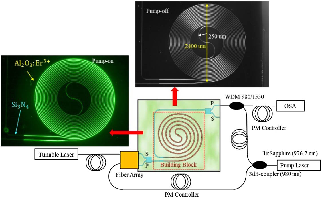
Figure 5 shows the experimental setup for the characterization of the net gain. The pump light at 976.2 nm is provided by a Ti:sapphire laser (700–1100 nm, Spectra-Physics Model 3900S). The signal light at 1460–1640 nm comes from a tunable laser with an integrated attenuation functionality (Agilent 8164B Lightwave measurement system with 81600B-201 laser module). TE polarization was used for the signal. The pump is split by a 3 dB coupler (PN980R5F1) and launched into both sides of the chip. This bidirectional pumping scheme helps invert the integrated Al2O3:Er3+ spiral more uniformly throughout its length. It also avoids the depletion of the pump by excited-state absorption of the pump at the beginning of the amplifier due to the high pump intensity required to invert the length of the amplifier if the pump was injected only by one side. On the left side, i.e., the input of signal light, the pump and signal are launched through different channels of a fiber array (127 μm pitch). They are multiplexed by the on-chip 2×1 MMI [40]. At the right side, after the 3 dB coupler, the pump passes first through the polarization-maintaining wavelength-division multiplexer (980/1550 WDM, WP9850F), and then is launched into the pump port of the on-chip 1×2 MMI demultiplexer. At the output, the residual pump and the amplified signal are further demultiplexed by an external WDM with the same type. The insertion losses of the external WDM coupler are 0.53 dB and 0.67 dB for the signal and pump, respectively. Eventually, the signal is connected to the optical spectrum analyzer (OSA) (HP 70950B) with a spectral resolution of 0.5 nm.

Fig. 5. Experimental setup utilized for the measurement of the net gain on the Al2O3:Er3+-Si3N4 integrated spiral amplifier. The pump light, at 976.2 nm, is split by a 3 dB coupler (operating wavelength 980 nm) and injected into the amplifier chip from both the input and output sides via MMI multi/demultiplexers. The signal, from a tunable laser operating in the C-band, is injected from the left and collected on the right side and directed to the optical spectrum analyzer. The photographs represent the integrated spiral amplifier in the pump-on and pump-off cases. The pitch between adjacent loops of the Al2O3:Er3+ spiral is 40 μm.

下载图片 查看所有图片

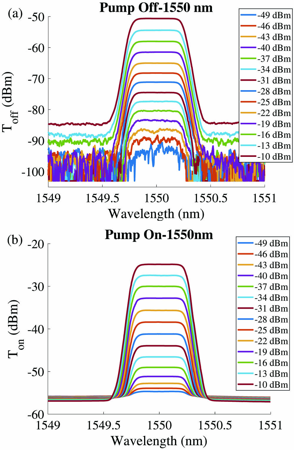
The ASE was subtracted from the signal spectra prior to the calculation of the signal enhancement using a similar method presented in Ref. [23]. The transmission spectrum collected by the OSA under the pump-off is Toff. When the pump is on, the spectrum of the amplified signal power (Ton) includes the ASE power which equals to the background power from the spectral curves (Tonb). For instance, Figs. 6(a) and 6(b) demonstrate the measured spectra under pump-off and pump-on cases at the wavelength of 1550 nm for different launched signal powers. When the pump is on, the background spectral power rises to about 57  dBm due to the ASE. To remove the ASE from the measured spectra, the peak power extracted from the amplified signal power first excludes the ASE background power Tonb. Therefore, Eq. (2) for the net Si3N4-to-Si3N4 gain extraction can be modified as

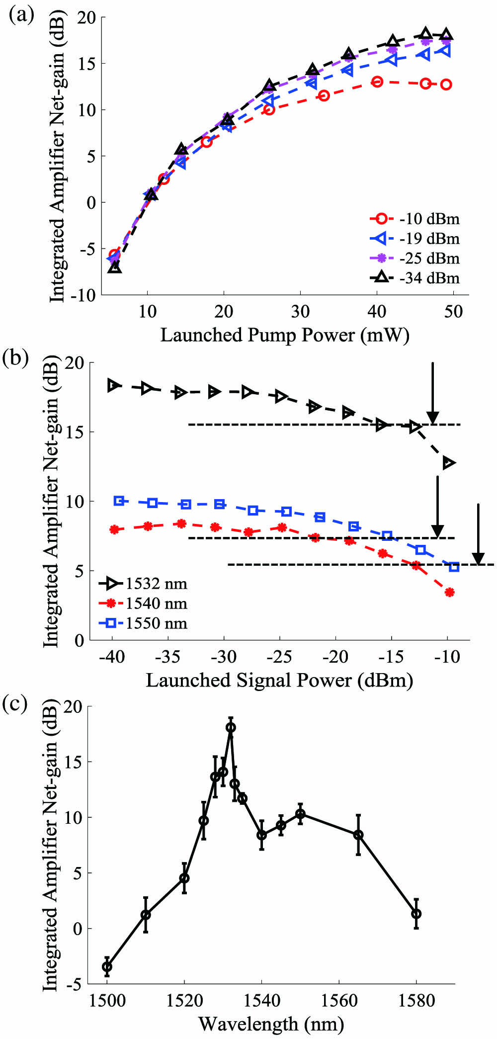
Figure 7(a) shows the net gain of the integrated amplifier after excluding the ASE as a function of the launched pump power. With increasing pump power, first, the net gain at different levels of launched signal rises rapidly and then saturates due to the bleaching of the ground state as a large amount of the active ions are excited. By setting the launched pump power to 50  mW, the net gain as a function of the launched signal power is presented in Fig. 7(b). Gain saturation effects occur when the launched signal power is larger than 13  dBm at 1532 nm, 1540 nm, and 1550 nm, which originates from the reduction of the excited ion density by stimulated emission. Furthermore, the net gain at other wavelengths from the telecommunication bands, i.e., S-band, C-band, and L-band, is characterized for a launched signal power of 30  dBm, as shown in Fig. 7(c). The monolithically integrated amplifier exhibits net gain within a bandwidth of 1510–1580 nm. A maximum net gain of 18.1±0.9  dB has been obtained at 1532 nm. This means that the Al2O3:Er3+ amplifier itself produces a net gain of 19  dB (i.e., excluding the adiabatic coupler losses), indicating a net gain per unit length of 1.97 dB/cm under bidirectional pumping. Assuming a 1.4 dB/cm propagation loss for the pump light, we simulated the optical gain of 19.5  dB at the wavelength of 1532 nm by using a similar rate-equation model and the spectroscopic parameters from the work of Ref. [36]. The experimental data has good agreement with this simulation value. Nevertheless, further modeling the gain requires locally characterized parameters for the rate-equation model.

Fig. 6. Measured spectra from the OSA at the wavelength of 1550 nm under (a) pump-off case and (b) pump-on case. The legend indicates the launched signal powers. The launched pump power is 50  mW.
下载图片 查看所有图片

Fig. 7. Net gain measurements. (a) Net gain of the integrated amplifier as a function of launched pump power for different launched signal powers (1532 nm of wavelength). (b) Net gain as a function of launched signal power for three different wavelengths within the C-band. The launched pump power is 50 mW. The dashed lines indicate 3 dB drop from the maximum gains for the three wavelengths. (c) Net gain as a function of wavelength for a launched signal power of 30 dBm and launched pump power of 50 mW. A bidirectional pumping scheme is applied. The reported launched power corresponds to the sum of the powers launched in each of the two input ports.

下载图片 查看所有图片

3. CONCLUSION

As a summary, we demonstrated an Al2O3:Er3+ amplifier monolithically integrated in Si3N4 technology. By using a simple double-layer photonic platform, active photonics are enabled in the Si3N4 platform via a scalable wafer-scale process. A net Si3N4-to-Si3N4 gain of 18.1±0.9  dB was obtained for a spiral length of 10 cm. The results are comparable to the highest net gain in a non-integrated Al2O3:Er3+ amplifier from previous work in our group [36]. A broad bandwidth net gain operation over 70 nm wavelength was also demonstrated. These results show the potential for monolithic integration of high optical gain in Si3N4 photonics, empowering applications such as data transmission, optical computing, quantum technology, and lidar chips for autonomous driving applications, for which on-chip optical gain is required.

4 Acknowledgment

Acknowledgment. The authors would like to thank LioniX International, Michiel de Goede, and Sergio Vázquez-Córdova for useful supports and discussions.

References

[1] F. Kish, V. Lal, P. Evans, S. W. Corzine, M. Ziari, T. Butrie, M. Reffle, H. S. Tsai, A. Dentai, J. Pleumeekers, M. Missey, M. Fisher, S. Murthy, R. Salvatore, P. Samra, S. Demars, N. Kim, A. James, A. Hosseini, P. Studenkov, M. Lauermann, R. Going, M. Lu, J. Zhang, J. Tang, J. Bostak, T. Vallaitis, M. Kuntz, D. Pavinski, A. Karanicolas, B. Behnia, D. Engel, O. Khayam, N. Modi, M. R. Chitgarha, P. Mertz, W. Ko, R. Maher, J. Osenbach, J. T. Rahn, H. Sun, K. T. Wu, M. Mitchell, D. Welch. System-on-chip photonic integrated circuits. IEEE J. Sel. Top. Quantum Electron., 2018, 24: 6100120.

[2] H. Subbaraman, X. Xu, A. Hosseini, X. Zhang, Y. Zhang, D. Kwong, R. T. Chen. Recent advances in silicon-based passive and active optical interconnects. Opt. Express, 2015, 23: 2487-2511.

[3] E. Lim, J. Song, Q. Fang, C. Li, X. Tu, N. Duan, K. K. Chen, R. P. Tern, T. Liow. Review of silicon photonics foundry efforts. IEEE J. Sel. Top. Quantum Electron., 2014, 20: 405-416.

[4] J. C. Hulme, J. K. Doylend, J. E. Bowers. Widely tunable Vernier ring laser on hybrid silicon. Opt. Express, 2013, 21: 19718-19722.

[5] E. Kasper, M. Kittler, M. Oehme, T. Arguirov. Germanium tin: silicon photonics toward the mid-infrared [Invited]. Photon. Res., 2013, 1: 69-76.

[6] P. Muñoz, G. Micó, L. Bru, D. Pastor, D. Pérez, J. Doménech, J. Fernández, R. Baños, B. Gargallo, R. Alemany, A. Sánchez, J. Cirera, R. Mas, C. Domínguez. Silicon nitride photonic integration platforms for visible, near-infrared and mid-infrared applications. Sensors, 2017, 17: 2088.

[7] D. J. Blumenthal, R. Heideman, D. Geuzebroek, A. Leinse, C. Roeloffzen. Silicon nitride in silicon photonics. Proc. IEEE, 2018, 106: 2209-2231.

[8] C. G. H. Roeloffzen, L. Zhuang, C. Taddei, A. Leinse, R. G. Heideman, P. W. L. van Dijk, R. M. Oldenbeuving, D. A. I. Marpaung, M. Burla, K.-J. Boller. Silicon nitride microwave photonic circuits. Opt. Express, 2013, 21: 22937-22961.

[9] L. Gaeta, M. Lipson, T. J. Kippenberg. Photonic-chip-based frequency combs. Nat. Photonics, 2019, 13: 158-169.

[10] Z. Subramanian, E. Ryckeboer, A. Dhakal, F. Peyskens, A. Malik, B. Kuyken, H. Zhao, S. Pathak, A. Ruocco, A. De Groote, P. Wuytens, D. Martens, F. Leo, W. Xie, U. D. Dave, M. Muneeb, P. Van Dorpe, J. Van Campenhout, W. Bogaerts, P. Bienstman, N. Le Thomas, D. Van Thourhout, Z. Hens, G. Roelkens, R. Baets. Silicon and silicon nitride photonic circuits for spectroscopic sensing on-a-chip [Invited]. Photon. Res., 2015, 3: B47-B59.

[11] C. Taballione, T. A. W. Wolterink, J. Lugani, A. Eckstein, B. A. Bell, R. Grootjans, I. Visscher, D. Geskus, C. G. H. Roeloffzen, J. J. Renema, I. A. Walmsley, P. W. H. Pinkse, K.-J. Boller. 8×8 reconfigurable quantum photonic processor based on silicon nitride waveguides. Opt. Express, 2019, 27: 26842-26857.

[12] V. Poulton, M. J. Byrd, M. Raval, Z. Su, N. Li, E. Timurdogan, D. Coolbaugh, D. Vermeulen, M. R. Watts. Large-scale silicon nitride nanophotonic phased arrays at infrared and visible wavelengths. Opt. Lett., 2017, 42: 21-24.

[13] B. Stern, X. Ji, A. Dutt, M. Lipson. Compact narrow-linewidth integrated laser based on a low-loss silicon nitride ring resonator. Opt. Lett., 2017, 42: 4541-4544.

[14] Y. Fan, J. P. Epping, R. M. Oldenbeuving, C. G. H. Roeloffzen, M. Hoekman, R. Dekker, R. G. Heideman, P. J. M. van der Slot, K. J. Boller. Optically integrated InP-Si3N4 hybrid laser. IEEE Photonics J., 2016, 8: 1505111.

[15] Y. Lin, C. Browning, R. B. Timens, D. H. Geuzebroek, C. G. H. Roeloffzen, M. Hoekman, D. Geskus, R. M. Oldenbeuving, R. G. Heideman, Y. Fan, K. J. Boller, L. P. Barry. Characterization of hybrid InP-triplex photonic integrated tunable lasers based on silicon nitride (Si3N4/SiO2) microring resonators for optical coherent system. IEEE Photonics J., 2018, 10: 1400108.

[16] C. G. H. Roeloffzen, M. Hoekman, E. J. Klein, L. S. Wevers, R. B. Timens, D. Marchenko, D. Geskus, R. Dekker, A. Alippi, R. Grootjans, A. van Rees, R. M. Oldenbeuving, J. P. Epping, R. G. Heideman, K. Wörhoff, A. Leinse, D. Geuzebroek, E. Schreuder, P. W. L. van Dijk, I. Visscher, C. Taddei, Y. Fan, C. Taballione, Y. Liu, D. Marpaung, L. Zhuang, M. Benelajla, K. J. Boller. Low-loss Si3N4 triplex optical waveguides: technology and applications overview. IEEE J. Sel. Top. Quantum Electron., 2018, 24: 4400321.

[17] O. de Beeck, B. Haq, L. Elsinger, A. Gocalinska, E. Pelucchi, B. Corbett, G. Roelkens, B. Kuyken. Heterogeneous III-V on silicon nitride amplifiers and lasers via microtransfer printing. Optica, 2020, 7: 386-393.

[18] M. Belt, T. Huffman, M. L. Davenport, W. Li, J. S. Barton, D. J. Blumenthal. Arrayed narrow linewidth erbium-doped waveguide-distributed feedback lasers on an ultra-low-loss silicon-nitride platform. Opt. Lett., 2013, 38: 4825-4828.

[19] J. D. B. Bradley, E. S. Hosseini, , Z. Su, T. N. Adam, G. Leake, D. Coolbaugh, M. R. Watts. Monolithic erbium- and ytterbium-doped microring lasers on silicon chips. Opt. Express, 2014, 22: 12226-12237.

[20] G. Singh, , J. D. B. Bradley, N. Li, E. S. Magden, M. Moresco, T. N. Adam, G. Leake, D. Coolbaugh, M. R. Watts. Resonant pumped erbium-doped waveguide lasers using distributed Bragg reflector cavities. Opt. Lett., 2016, 41: 1189-1192.

[21] , N. Li, E. S. Magden, G. Singh, N. Singh, A. Baldycheva, E. S. Hosseini, J. Sun, M. Moresco, T. N. Adam, G. Leake, D. Coolbaugh, J. D. B. Bradley, M. R. Watts. Ultra-narrow-linewidth Al2O3:Er3+ lasers with a wavelength-insensitive waveguide design on a wafer-scale silicon nitride platform. Opt. Express, 2017, 25: 13705-13713.

[22] N. Li, D. Vermeulen, Z. Su, E. S. Magden, M. Xin, N. Singh, A. Ruocco, J. Notaros, C. V. Poulton, E. Timurdogan, C. Baiocco, M. R. Watts. Monolithically integrated erbium-doped tunable laser on a CMOS-compatible silicon photonics platform. Opt. Express, 2018, 26: 16200-16211.

[23] J. Rönn, W. Zhang, A. Autere, X. Leroux, L. Pakarinen, C. Alonso-Ramos, A. Säynätjoki, H. Lipsanen, L. Vivien, E. Cassan, Z. Sun. Ultra-high on-chip optical gain in erbium-based hybrid slot waveguides. Nat. Commun., 2019, 10: 432.

[24] R. C. Figueiredo, N. S. Ribeiro, A. M. O. Ribeiro, C. M. Gallep, E. Conforti. Hundred-picoseconds electro-optical switching with semiconductor optical amplifiers using multi-impulse step injection current. J. Lightwave Technol., 2015, 33: 69-77.

[25] M. Pollnau. Rare-earth-ion-doped channel waveguide lasers on silicon. IEEE J. Sel. Top. Quantum Electron., 2015, 21: 414-425.

[26] R. Soulard, A. Zinoviev, J. L. Doualan, E. Ivakin, O. Antipov, R. Moncorgé. Detailed characterization of pump-induced refractive index changes observed in Nd:YVO4, Nd:GdVO4 and Nd:KGW. Opt. Express, 2010, 18: 1553-1568.

[27] J. D. B. Bradley, M. Costa de Silva, M. Gay, L. Bramerie, A. Driessen, K. Wörhoff, J.-C. Simon, M. Pollnau. 170 Gbit/s transmission in an erbium-doped waveguide amplifier on silicon. Opt. Express, 2009, 17: 22201-22208.

[28] D. Geskus, S. Aravazhi, S. M. García-Blanco, M. Pollnau. Giant optical gain in a rare-earth-ion-doped microstructure. Adv. Mater., 2012, 24: OP19-OP22.

[29] M. A. Sefunc, F. B. Segerink, S. M. García-Blanco. High index contrast passive potassium double tungstate waveguides. Opt. Mater. Express, 2018, 8: 629-638.

[30] A. Aghajani, G. S. Murugan, N. P. Sessions, V. Apostolopoulos, J. S. Wilkinson. Waveguide lasers in ytterbium-doped tantalum pentoxide on silicon. Opt. Lett., 2015, 40: 2549-2552.

[31] H. C. Frankis, H. M. Mbonde, D. B. Bonneville, C. Zhang, R. Mateman, A. Leinse, J. D. B. Bradley. Erbium-doped TeO2-coated Si3N4 waveguide amplifiers with 5 dB net gain. Photon. Res., 2020, 8: 127-134.

[32] K. M. Kiani, H. C. Frankis, H. M. Mbonde, R. Mateman, A. Leinse, A. P. Knights, J. D. B. Bradley. Thulium-doped tellurium oxide waveguide amplifier with 7.6 dB net gain on a silicon nitride chip. Opt. Lett., 2019, 44: 5788-5791.

[33] H. Penilla, L. F. Devia-Cruz, M. A. Duarte, C. L. Hardin, Y. Kodera, J. E. Garay. Gain in polycrystalline Nd-doped alumina: leveraging length scales to create a new class of high-energy, short pulse, tunable laser materials. Light Sci. Appl., 2018, 7: 33.

[34] J. D. B. Bradley, M. Pollnau. Erbium-doped integrated waveguide amplifiers and lasers. Laser Photonics Rev., 2011, 5: 368-403.

[35] N. Li, E. S. Magden, Z. Su, N. Singh, A. Ruocco, M. Xin, M. Byrd, P. T. Callahan, J. D. B. Bradley, C. Baiocco, D. Vermeulen, M. R. Watts. Broadband 2-μm emission on silicon chips: monolithically integrated holmium lasers. Opt. Express, 2018, 26: 2220-2230.

[36] S. A. Vázquez-Córdova, M. Dijkstra, E. H. Bernhardi, F. Ay, K. Wörhoff, J. L. Herek, S. M. García-Blanco, M. Pollnau. Erbium-doped spiral amplifiers with 20 dB of net-gain on silicon. Opt. Express, 2014, 22: 25993-26004.

[37] E. H. Bernhardi, H. A. G. M. van Wolferen, L. Agazzi, M. R. H. Khan, C. G. H. Roeloffzen, K. Wörhoff, M. Pollnau, R. M. de Ridder. Ultra-narrow-linewidth, single-frequency distributed feedback waveguide laser in Al2O3:Er3+ on silicon. Opt. Lett., 2010, 35: 2394-2396.

[38] J. Mu, M. Dijkstra, Y. Yong, M. de Goede, L. Chang, S. M. García-Blanco. Monolithic integration of Al2O3 and Si3N4 toward double-layer active-passive platform. IEEE J. Sel. Top. Quantum Electron., 2019, 25: 8200911.

[39] J. Mu, M. Dijkstra, S. M. García-Blanco. Resonant coupling for active-passive monolithic integration of Al2O3 and Si3N4. IEEE Photonics Technol. Lett., 2019, 31: 771-774.

[40] J. Mu, S. A. Vázquez-Córdova, M. A. Sefunc, Y.-S. Yong, S. M. García-Blanco. A low-loss and broadband MMI-based multi/demultiplexer in Si3N4/SiO2 technology. J. Lightwave Technol., 2016, 34: 3603-3609.

[41] J. D. B. Bradley, L. Agazzi, D. Geskus, F. Ay, K. Wörhoff, M. Pollnau. Gain bandwidth of 80 nm and 2 dB/cm peak gain in Al2O3:Er3+ optical amplifiers on silicon. J. Opt. Soc. Am. B, 2010, 27: 187-196.

[42] Y. Okamura, S. Yoshinaka, S. Yamamoto. Measuring mode propagation losses of integrated optical waveguides: a simple method. Appl. Opt., 1983, 22: 3892-3894.

Jinfeng Mu, Meindert Dijkstra, Jeroen Korterik, Herman Offerhaus, Sonia M. García-Blanco. High-gain waveguide amplifiers in Si3N4 technology via double-layer monolithic integration[J]. Photonics Research, 2020, 8(10): 10001634.

本文已被 3 篇论文引用
被引统计数据来源于中国光学期刊网
引用该论文: TXT   |   EndNote

相关论文

加载中...

关于本站 Cookie 的使用提示

中国光学期刊网使用基于 cookie 的技术来更好地为您提供各项服务,点击此处了解我们的隐私策略。 如您需继续使用本网站,请您授权我们使用本地 cookie 来保存部分信息。
全站搜索
您最值得信赖的光电行业旗舰网络服务平台!