Photonics Research, 2017, 5 (2): 02000108, Published Online: Sep. 26, 2018  

Compact, submilliwatt, 2 × 2 silicon thermo-optic switch based on photonic crystal nanobeam cavities

Author Affiliations
1 State Key Lab of Advanced Optical Communication Systems and Networks, Department of Electronic Engineering, Shanghai Jiao Tong University, Shanghai 200240, China
2 Engineering Department, University of Massachusetts, Boston, Massachusetts 02125, USA
3 e-mail: qiuciyuan@sjtu.edu.cn
4 e-mail: yikaisu@sjtu.edu.cn
Figures & Tables

Fig. 1. (a) Schematic diagram of the proposed 2×2 TO switch based on dual PCN cavities. The phase difference between the two arms (Φ1Φ2) is equal to π. (b) Cross-section view of the coupled region in one half of the proposed 2×2 TO switch.

下载图片 查看原文

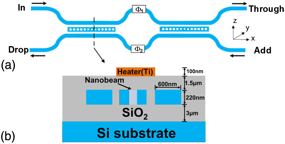
Fig. 2. (a) Calculated electric field distribution of a single PCN 3W structure at the resonant wavelength based on 2.5D variational FDTD simulation. (b) Simulated transmission spectra of a single PCN 3W structure.

下载图片 查看原文

Fig. 3. (a) Micrograph of the fabricated 2×2 TO switch based on dual PCN 3W structures. (b) SEM image of the fabricated PCN 3W structure. (c) Device after wire bonding to a PCB.

下载图片 查看原文

Fig. 4. Transmission spectra of a fabricated single PCN 3W structure in through (red solid), drop (green solid), and add (blue dash) ports. Note that the transmissions are normalized to a reference waveguide and the same to the below measured transmission spectra.

下载图片 查看原文

Fig. 5. (a) Transmission spectra of the fabricated 2×2 TO switch based on dual PCN 3W structures with the unaligned wavelength state (solid lines) and the aligned wavelength state (lines with symbols). (b) Transmission spectra of the fabricated 2×2 TO switch based on dual PCN 3W structures with a π phase difference at through (red line)/drop (blue line)/add (green line) ports.

下载图片 查看原文

Fig. 6. (a) Transmission spectra of the fabricated 2×2 TO switch based on dual PCN 3W structures with various applied powers (P1,P2,P3) at the through ports (solid lines) and the drop ports (lines with symbols). (b) Fitting curve of the resonance wavelength shift of 2×2 TO switch based on dual PCN 3W structures as a function of the applied power.

下载图片 查看原文

Table1. Comparisons of the Operation Performances of Various Silicon TO Switches

TypesDevice FootprintThermal Tuning EfficiencySwitching Power
Adiabatic bend-based MZI [28]5000  μm212.7 mW
MRR [29]400  μm20.25 nm/mW3.3 mW
MZI [30]>10000  μm230 mW
Dual MRRs [31]1000  μm20.9 nm/mW6.8 mW
Photonic crystal [32]35  μm×10  μm0.63 nm/mW18.2 mW
2D waveguide-based MZI [33]42  μm×42  μm26 mW
Our work30  μm×150  μm1.23 nm/mW0.16 mW

查看原文

Huanying Zhou, Ciyuan Qiu, Xinhong Jiang, Qingming Zhu, Yu He, Yong Zhang, Yikai Su, Richard Soref. Compact, submilliwatt, 2 × 2 silicon thermo-optic switch based on photonic crystal nanobeam cavities[J]. Photonics Research, 2017, 5(2): 02000108.

引用该论文: TXT   |   EndNote

相关论文

加载中...

关于本站 Cookie 的使用提示

中国光学期刊网使用基于 cookie 的技术来更好地为您提供各项服务,点击此处了解我们的隐私策略。 如您需继续使用本网站,请您授权我们使用本地 cookie 来保存部分信息。
全站搜索
您最值得信赖的光电行业旗舰网络服务平台!