Photonics Research, 2019, 7 (10): 10001127, Published Online: Sep. 9, 2019
Monolithic integration of MoS2-based visible detectors and GaN-based UV detectors  Download: 740次
Figures & Tables
Fig. 1. (a) Illustration of the SL MoS 2 MoS 2 MoS 2
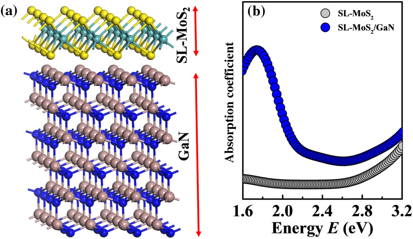
Fig. 2. (a) Illustration of SL MoS 2 MoS 2 MoS 2 MoS 2 MoS 2 ∼ 0.7 nm MoS 2 MoS 2

Fig. 3. (a) Schematic diagram of the preparation steps of monolithic integration of GaN-based UV detectors and MoS 2 MoS 2 MoS 2 / GaN 1 cm × 1 cm

Fig. 4. (a) Dark current and light current for 280 nm incident light under different powers of the GaN PD. (b) Dark current and light current for a 405 nm laser under different incident powers of the MoS 2

Fig. 5. (a) Responsivity R G D * R G D * MoS 2

Fig. 6. Photocurrent as a function of time under alternative dark and illumination. (a) Photocurrent-time curve of GaN illuminated by a 280 nm light source with the incident power of 15.01 nW at 20 V. (b) The rise time (from 10% to 90% of maximum photocurrent) and the fall time (from 90% to 10% of maximum photocurrent) of the GaN PD. (c) Photocurrent-time curve of MoS 2 / GaN MoS 2 / GaN

You Wu, Zhiwen Li, Kah-Wee Ang, Yuping Jia, Zhiming Shi, Zhi Huang, Wenjie Yu, Xiaojuan Sun, Xinke Liu, Dabing Li. Monolithic integration of MoS2-based visible detectors and GaN-based UV detectors[J]. Photonics Research, 2019, 7(10): 10001127.


 PDF全文
PDF全文

