1. INTRODUCTION
Future optical interconnect systems needed high-speed, low-power, and low-cost optical components to meet the demands of rapidly growing data communication. Si-based photonics was a promising technology for this application [1], as it is highly compatible with Si complementary metal–oxide–semiconductor (CMOS) technology. Basic devices of the Si photonics such as high-speed photodetectors [24" target="_self" style="display: inline;">–4], modulators [5–8" target="_self" style="display: inline;">–8], and many passive components [9] have been widely studied. Among these devices, the modulator was the key device that largely determines the quality of the transmitting signal in optical links. Due to the weak electro-optical effect, most high-speed Si modulators were demonstrated by using free carrier dispersion effects in the phase-shift structure. Si modulators with a Mach–Zehnder interferometer could realize high-speed modulation, broad optical bandwidth, and robust thermal tolerance [7]. But, they suffered from large footprints on the order of , which incur relatively high power consumption. The footprint and power consumption of the Si modulators could be reduced dramatically by using ring or photonic crystal configuration [5]. However, this improvement was obtained on the sacrifice of optical bandwidth, thermal tolerance, and fabrication tolerance [8]. To balance these parameters, Ge or GeSi electro-absorption modulators (EAMs) based on the Franz–Keldysh (FK) effect have emerged [10–15" target="_self" style="display: inline;">–15]. Recently, 56 Gbps high-speed Ge and GeSi EAMs with lateral p-i-n or wrap-around p-i-n structure were demonstrated [13,14]. Some of these EAMs even had the capability of transmitting single-lane 100 Gbps [15]. However, the fabrication processes of these EAMs were very complex. Some EAMs required chemical–mechanical polish (CMP) of Ge and extra poly-Si tapers [13,15], and other EAMs needed several precise Ge etchings [11,12,14].
In this paper, we presented a novel evanescently-coupled high-speed Ge waveguide EAM on 220-nm-thick silicon-on-insulator (SOI) platform. The fabrication processes of the EAM were simple. The Ge waveguide with two Ge tapers of the EAM was selectively grown on a Si waveguide. Neither CMP nor Ge etching was necessary. An asymmetric p-i-n junction was employed to change the electric field intensity of the Ge layer for the FK effect. The static characteristics including dark current, optical responsivity, insertion loss (IL), dc extinction ratio (ER), and power consumption were studied. The electro-optic 3 dB bandwidth, modulated bit rate, and dynamic power consumption exhibited the high-speed performance of the Ge EAM.
2. DESIGN AND FABRICATION
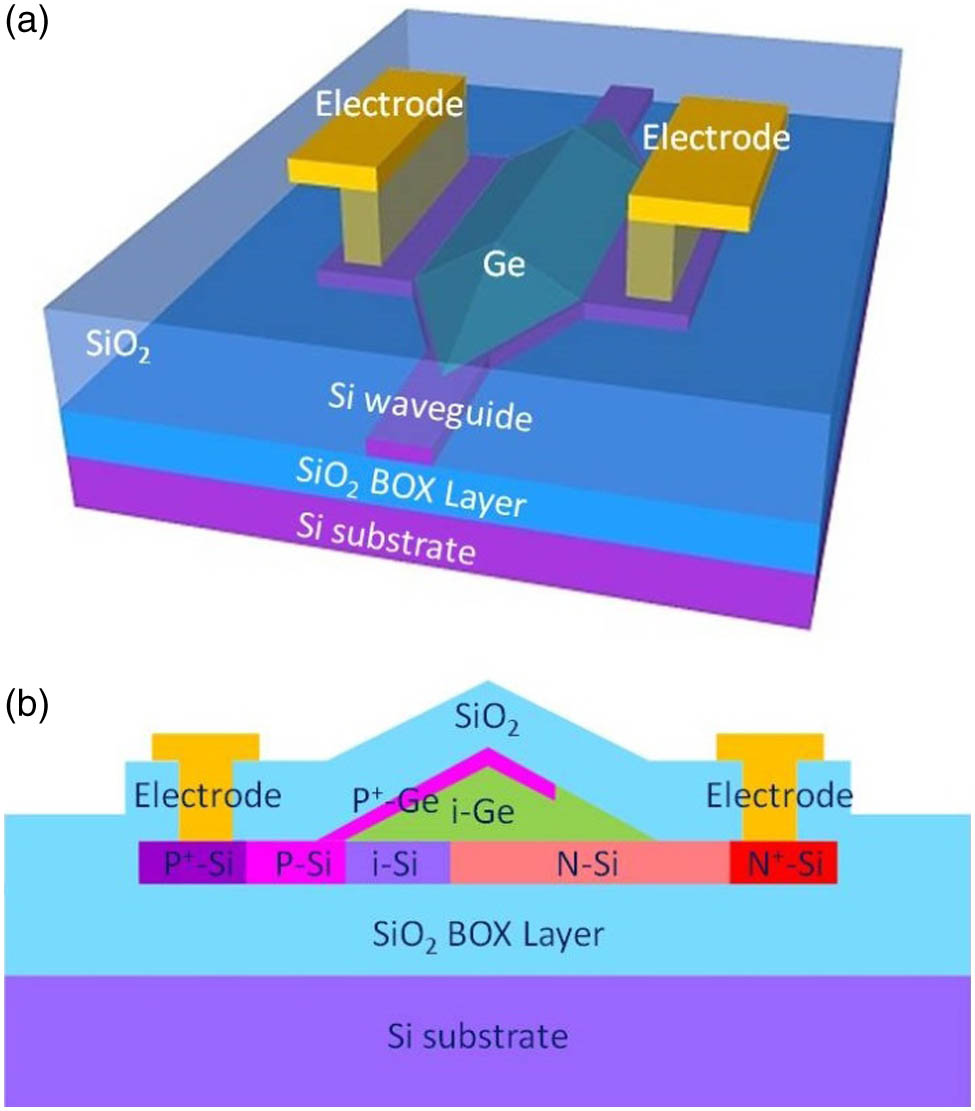
Figure 1(a) shows a schematic view of our EAM. The light came from the input Si waveguide and evanescently coupled into/out of the EAM through three-dimensional Ge tapers. A similar structure was demonstrated for a high-responsivity Ge photodetector [16]. The cross-sectional shapes of the Ge tapers and waveguide were isosceles triangles. The shape of the Ge depended on growth conditions. Moderate growth temperature and low growth pressure would lead the triangle with a 25° angle, which corresponded to the (113) face of the Ge [4]. In the EAM, an asymmetric p-i-n junction was introduced to apply a reverse field, which was needed for changing the absorption coefficient in Ge by the FK effect. Figure 1(b) shows the schematic cross-sectional shape and doping of the Ge EAM. , P-Si, i-Si, N-Si, and were defined in the top Si layer of the SOI. One side of the Ge contacted with P-Si, and another side of the Ge was on the N-Si. Part of the top Ge was doped, which adjoined the P-Si. The asymmetric p-i-n junction in Ge was formed by , i-Ge, and N-Si. Two electrodes were on the heavy-doped Si and far from Ge waveguide to avoid optical loss.
Fig. 1. (a) Schematic view of the EAM, (b) schematic cross-sectional structure of the EAM.
下载图片 查看所有图片
The optical transmission and field distribution of the EAM were simulated by finite-difference time-domain (FDTD) simulation. Figure 2(a) exhibited the cross-sectional optical field distribution of the EAM. Although the width of the Ge waveguide was 2 μm, most of the optical field was confined in the center of the Ge waveguide within , due to the relatively flat triangle structure. The fundamental TE mode loss of the structure of the device (no material absorption was included) was lower than 0.12 dB within 1570–1630 nm [Fig. 2(b)], which indicated efficient optical coupling. The inset of Fig. 2(b) was the optical field distribution of the light (1610 nm), which coupled into/out of the EAM. A smooth optical field also suggested low mode loss. Figure 2(c) shows the electric field distribution in the EAM at . The electric field and the optical field in the EAM overlapped each other very well, which was the requirement of highly efficient modulation. Extracted electric field distributions at the center of the Ge waveguide at 0 V and are shown in Fig. 2(d). The average electric field intensity at 0 V was about 25 kV/cm at the center of the Ge waveguide. It increased to about 80 kV/cm at , which could provide a strong FK effect in the EAM.
Fig. 2. (a) Cross-sectional optical field distribution of the EAM, (b) loss of the fundamental TE mode of the device’s structure, (c) electric field distribution in the EAM at , and (d) extracted electric field distributions at the center of the Ge waveguide at 0 V and . The inset of (b) is the optical field distribution of the light (1610 nm) coupling into/out of the EAM.
下载图片 查看所有图片
The devices started on an SOI substrate with a 220-nm-thick Si(001) top layer and a 2-μm-thick buried oxide (BOX) layer. Grating couplers and waveguides were fabricated by deep ultraviolet (DUV) lithography and dry etching. The width of the input/output Si waveguide was 450 nm. In the EAM region, the width and length of the rectangular Si layer were 15 μm and 30–60 μm, respectively. Between the input/output Si waveguide and the rectangular Si layer, there were two 5 μm long Si tapers, which changed the Si waveguide width from 450 nm to 2 μm. The Si layer in the EAM region was implanted to form , P-Si, N-Si, and , respectively. Intrinsic Ge was selectively grown on the Si waveguide and connected to the P-Si, i-Si, and N-Si. The width and the height of the epitaxial Ge on Si layer were 2 and 0.5 μm, respectively. The length of the Ge varied from 40 to 70 μm. Due to the nature of selective growth, the three-dimensional Ge tapers were formed naturally in the both ends of the EAM without further complex fabrication processes such as CMP or Ge etching. Then, part of the top Ge was implanted to realize , which was in contact with the P-Si. Finally, metal electrodes were fabricated on the and to form good Ohmic contacts. The devices were fabricated in the CompoundTek Si photonics platform with the smallest Si waveguide critical dimension of 90 nm. Figure 3(a) shows the top-view optical micrograph of the EAMs. The grating couplers and waveguide without EAM for IL comparison are also shown in the upper part of the Fig. 3(a). The cross-sectional scanning electron microscope (SEM) image of the EAM is shown in Fig. 3(b). Although the shape of the Ge waveguide was not a strict triangle with 25° angles, the shape was similar to the structure in the previous simulation.
Fig. 3. (a) Top-view optical micrograph of the EAMs, (b) cross-sectional SEM image of the EAM.
下载图片 查看所有图片
3. RESULTS AND DISCUSSION
The current-voltage (I-V) characteristics of the EAM with/without light incidence were obtained by using an Agilent B1500A semiconductor parameter analyzer, a probe station, and a Santec tunable laser TSL-550 (1500–1630 nm) at room temperature. Figure 4 shows the typical I-V curve of the EAM from 1 V to . The length of the device was 40 μm. The device exhibited a very good rectifying behavior with a high on/off current ratio near between 1 and . The dark current of the device was only 6 nA and 12 nA at and , respectively. Such good I-V curves indicated the high quality of the Ge and asymmetric p-i-n junction. The I-V curve of the device under the light incidence is shown in Fig. 4. The incident light was coupled into the EAM from a grating coupler by a single-mode fiber. The wavelength and input optical power of the incident light were 1610 nm and 1 mW, respectively. The optical responsivity of the EAM at 1610 nm was 0.49 A/W at 0 V. It significantly increased with the reverse bias, which suggested a strong FK effect in the EAM. The responsivity increased to 0.73 A/W at . The capacitance-voltage (C-V) characteristic of the EAM was measured by the Agilent B1500A semiconductor parameter analyzer at 1 MHz. The C-V curve is also shown in Fig. 4. The capacitance of the EAM was about 60 fF at 0 V. It decreased quickly from 0 V to , which indicated the expansion of depleted layer under bias voltage. When the reverse bias was lower than , the capacitance of the device trended to stabilize. The capacitance of the EAM was about 24 fF at , which was small enough to ensure a high bandwidth.
Fig. 4. Typical I-V curves (with or without light input) and C-V curve of the EAM.
下载图片 查看所有图片
The IL and ER were measured by the Santec tunable laser TSL-550, the Keithley 2611A, a commercial optical power meter, and a probe station. The input light and output light of the EAM were coupled via the optical coupling between grating couplers and single-mode fibers. The optical transmission loss (including coupling loss) of the EAM at 0 V to is shown in Fig. 5(a). The reference structure without the EAM also is shown for comparison. The optical loss of the reference structure contained the coupling loss of the same two grating couplers. Therefore, the coupling loss of the single grating coupler was about 6.7 dB at 1610 nm. The IL of the EAM could be calculated by subtracting the coupling loss. Figure 5(b) shows the IL and ER of the EAM from 1560 to 1630 nm. The IL decreased rapidly with the increasing of the wavelength, which was mainly attributed to the indirect band absorption and residual FK absorption. At 1610 nm, the IL was 6.2 dB. The IL was a little larger than that of the reported Ge EAM [12,13], which could be attributed to strong residual FK absorption induced by the high built-in electric field (25 kV/cm) at 0 V. Therefore, the IL of the device would be obviously reduced by suitably increasing the distance between and N-Si. The peak of the ER curve of the device appeared around 1600 nm, which was in good agreement with the FK effect of Ge. The ER of the device at 3 and 4 V swing was 3.8 (3.6) dB and 4.8 (4.6) dB at 1600 (1610) nm, respectively. Higher ER was observed in the longer EAMs, which resulted in higher IL.
Fig. 5. (a) Optical transmission loss of the EAM (at various bias voltages) and without EAM, (b) IL and dc ER curves (at various bias voltages) of the EAM.
下载图片 查看所有图片
The electro-optic bandwidth of the modulator was obtained by a 40 GHz vector network analyzer, a 50 Ω-terminated ground-signal-ground (GSG) RF probe, an Amonics conventional long (CL)-band Er-doped fiber amplifier (EDFA), a bias-tee, and a high-speed commercial photodetector. The electrical signal from the vector network analyzer and reverse voltage were applied to the EAM via the bias-tee and the 50 Ω-terminated GSG RF probe. Light from the tunable laser was coupled into the EAM, and the CL-band EDFA was used to amplify the modulated optical signal from the EAM. The amplified optical signal was introduced into the high-speed commercial photodetector to change the optical signal to the electrical signal. The electrical signal was fed to the vector network analyzer, where the S-parameters of the EAM were shown. Figure 6 shows the normalized electro-optic response (S21) of the EAM at various bias voltages. The electro-optic 3 dB bandwidth of the EAM was about 36 GHz at . The 3 dB bandwidth had no changes with bias voltage, which was in good agreement with the C-V curves of the EAM. Because the FK effect was a sub-picosecond phenomenon [17], the speed of the FK modulator was only limited by the resistor capacitor (RC) delay. When the bias voltage was lower than , like the capacitance of the device, the 3 dB bandwidth of the device was also trending to stabilize. The S11 curves of the EAM are also shown in Fig. 6. Like the S21 curves, the S11 curves have little change with the bias voltage. An equivalent circuit model (the inset in Fig. 6) was used for extracting the electrical parameters of the EAM. In the equivalent circuit model, was the capacitance of the BOX layer, was the resistance of the substrate, was the series resistance, was the junction capacitance, and was the capacitance of the pads. After the fitting, of 20 fF and of 205 Ω were obtained at , which indicated the RC-limited bandwidth of the EAM was about 39 GHz. This result was in good agreement of the experimental 3 dB bandwidth of the EAM.
Fig. 6. S21 and S11 curves of the EAM at various bias voltages. The inset is the equivalent circuit model of the EAM.
下载图片 查看所有图片
Eye diagrams were measured on the wafer to study the high-speed performance of the EAM. A 56 Gbps () non-return-to-zero (NRZ) pseudorandom binary sequence (PRBS) electrical signal was generated by a bit pattern generator. This electrical signal was amplified by an RF amplifier to the peak-to-peak voltage (Vpp) of 3 V, which was applied to the device via a bias-tee and a 50 Ω-terminated GSG RF probe. The reverse voltage, which adjusted the working condition of the EAM, was . The input power of the light was 1 mW. The CL-band EDFA was used to amplify the modulated optical signal from the EAM. The amplified optical signal was fed to a sampling oscilloscope, which was shown in the eye diagrams. Figure 7 shows the 56 Gbps eye diagrams of the EAM at 1600 and 1610 nm. Clear and open eye diagrams at 56 Gbps were observed. The dynamic ER of the device was 2.8 and 2.7 dB with the signal-to-noise ratio (SNR) larger than 5 for 1600 nm and 1610 nm, respectively. Similar eye diagrams at 1590 nm and 1620 nm with relatively low ER were also observed. The optical bandwidth of the EAM was larger than 30 nm. The dynamic ER would be improved by using an L-band tunable optical filter to clear the optical signal that comes from the EDFA.
Fig. 7. 56 Gbps eye diagrams of the EAM at 1600 and 1610 nm.
下载图片 查看所有图片
The power consumption of the EAM could be divided into static and dynamic power. The static power consumption of the EAM could be estimated as average current multiplied by bias voltage. The average current of the device was about 0.7 mA under 1 mW optical input (1610 nm) at the bias voltage of . Therefore, the static power of the EAM was about 1.2 mW. The dynamic power consumption per bit could be estimated by [13]. The Cj and the Vpp of the EAM were and , respectively. Thus, the dynamic power consumption of the device was 45 fJ/bit. For comparison, performances of the reported Ge or GeSi EAMs are shown in Table 1.
Table 1. Performance Comparison for Ge or GeSi EAMs
| Modulator Type | Refs. | SOI Platform (μm) | Footprint () | Wavelength (nm) | Voltage Swing (V) | Optical Bandwidth (nm) | 3 dB Bandwidth (GHz) | Energy per Bit (fJ/bit) | DC ER (dB) | IL (dB) | Dynamic ER (dB) | Max. Bit Rate (Gbps) | | GeSi EAM | [12] | 3 | | 1550 | 3 | | 38 | 147 | 5.9 | 4.8 | 4.5 | 28 | | Ge EAM | [13] | 0.22 | | 1615 | 2 | | | 12.8 | 4.6 | 4.9 | 3.3 | 56 | | GeSi EAM | [18] | 0.22 | | 1560 | 2 | 30 | | 13.8 | 4.2 | 4.4 | 3.0 | 50 | | GeSi EAM | [14] | 0.8 | | 1566 | 4 | / | 56 | 44 | 5.6 | 10.6 | 5.2 | 56 | | Ge EAM | This work | 0.22 | | 1610 | 3 | | 36 | 45 | 3.6 | 6.2 | 2.7 | 56 |
|
查看所有表
4. SUMMARY
In summary, high-speed evanescent-coupled Ge waveguide EAMs were demonstrated on an SOI platform with simple fabrication processes. The Ge waveguide was selectively grown on Si without further complex fabrication processes such as CMP and Ge etching. To adjust the isosceles triangle shape of the Ge waveguide, the asymmetric p-i-n junction was introduced into the Ge EAM. The device had low dark current and small capacitance. The IL and dc ER of the EAM at 1610 nm were 6.2 dB and 3.6 dB (voltage swing of ), respectively. The electro-optic bandwidth of the device was about 36 GHz at . Clear open eye diagrams were observed at 56 Gbps with a dynamic ER of 2.7 dB for voltage swing of . The EAM also had very low power consumption. The static and dynamic power consumption of the EAM was 1.2 mW and 45 fJ/bit, respectively. The device could work at the C-band by using suitable GeSi material instead of pure Ge layers. This EAM could have potential applications in Si-based on-chip optical interconnects with a small footprint and low-power consumption.
5 Acknowledgment
Acknowledgment. The authors thank Professor Lin Yang for his help in eye diagram measurements. The authors also thank Professor Zhiyong Li for considerable discussions.
Zhi Liu, Xiuli Li, Chaoqun Niu, Jun Zheng, Chunlai Xue, Yuhua Zuo, Buwen Cheng. 56 Gbps high-speed Ge electro-absorption modulator[J]. Photonics Research, 2020, 8(10): 10001648.
 Download: 715次


