Chinese Optics Letters, 2018, 16 (7): 070901, Published Online: Jul. 19, 2018  

Mode division multiplexed holography by out-of-plane scattering of plasmon/guided modes Download: 576次

Author Affiliations
National Laboratory of Solid State Microstructures, College of Engineering and Applied Sciences, Collaborative Innovation Center of Advanced Microstructures, Nanjing University, Nanjing 210093, China
Abstract
We design and demonstrate a type of multiplexed hologram by nanoscatterers inside a dielectric-loaded plasmonic waveguide with guided-wave illuminations. The mode division multiplexed hologram (MDMH) is fulfilled by the scattering of guided waves to free space with respect to different modes. According to different mode numbers, these guided modes have different responses to the multiplexed hologram, and then give rise to different holographic images in reconstructions. In experiments, we show two kinds of MDMHs based on TM0/TE0 and TE0/TE1 modes as examples. Our approach could enrich the holography method that favors on-chip integration.

Controlling light to transfer more information has always been the pursuit of people, not only in optical communications but also in imaging systems. Holography[1] is such a general approach in optical phenomena that enables the recording and reconstruction of the full amplitude and phase information of an object. With the invention of computer-generated holograms[2], people are able to create holograms of virtual objects that do not exist in reality. Compared with conventional holograms (e.g., by a spatial light modulator), the recently developed metasurface[316" target="_self" style="display: inline;">16] with subwavelength pixels is able to carry optical information with more flexible modulations in amplitude, phase, polarization, etc., and a wider field of view (FOV) that provides people with a superb hologram[1221" target="_self" style="display: inline;">21] with enhanced imaging performance. However, despite its ultra-thin advantage, a metasurface still needs external illumination from an outside light source, which is not conducive to its on-chip integration. A surface plasmon polariton (SPP) is a possible carrier for compact photonic integration due to its strong field confinement at the metal surface. Progress has been reported in its near-field manipulations such as focusing[22], a Bragg mirror[23], and beam engineering[2430" target="_self" style="display: inline;">30]. More recently, the near-field propagating SPP wave has also been engineered for free-space[31] beams and even holographic imaging[3234" target="_self" style="display: inline;">–34] by carefully designing the surface scatterers. It possibly indicates a kind of compact on-chip display devices. Nevertheless, the huge Ohmic loss of the plasmonic mode severely restricts its applications in large-area holograms. In addition, the singlet TM polarization nature of an SPP limits the capacity of multiple modes.

In fact, people have developed dielectric-loaded plasmonic waveguides (DLPWs) to optimize the mode confinement and propagation loss[35,36]. When the dielectric layer is thick enough, a DLPW is able to carry more guided modes, including the transverse electric (TE) field ones, which have less mode field inside the metal part and exhibit a much lower loss. Such a kind of mode demultiplexer has been demonstrated in in-plane mode focusing[35], which indicates a possible application of the out-of-plane hologram like the SPP does[31,34]. In this Letter, we extend the multiplexed hologram by SPP scattering to the DLPW in which both TM and TE and their higher-ordered modes can be used for scattering holography. Unlike the previous SPP propagation-dependent multiplexing[34], this new proposed mode division multiplexed hologram (MDMH) can generate multiple free-space images in the same input direction as the guided modes. Here, holographic images multiplexed both in TM/TE and TE0/TE1 modes are designed and demonstrated by well-arranged nanohole scatterings for proper guided-mode illuminations. Our approach provides a new dimension of multiplexed recording that enhances the information capacity.

First, it is necessary to introduce the diffraction process to manipulate the guided-mode holograms in the DLPW. A novel phase modulation method for propagating plane waves by in-plane diffractions from nonperiodic nanoarrays was first introduced in SPP systems[26]. By defining nanoscatterers at proper locations, the phase of the propagating field can be selected for the diffracted beam engineering, e.g., Airy SPP[26], collimated SPP[29,37], and winding SPP[30]. This in-plane diffraction method was further extended to out-of-plane beam engineering[31,38] and holography[34] on one hand and to mode division multiplexing (MDM) focusing in DLPW systems[35] on the other hand. Here, we incorporate the DLPW modes into multiplexed holograms by defining the corresponding phase evolution of the diffracted guided modes, which can be written as φobj(x,y)=φ0+kGM·l+2mπ,where φ0 is the constant initial phase of the guide wave, kGM is the wave vector of the guided mode, l is the propagating direction of the guided waves, m is the integer number, and φobj(x,y) is the required phase distribution for the hologram. From Eq. (1), it can be found that the phase evolution is closely related with the wave vector of the guided modes. Therefore, it is capable of recording information from multiple objects into a single hologram pattern.

Before getting into the experimental details, we need to analyze the mode properties in the DLPW. Figure 1(a) shows the calculated theoretical mode curve. It is evident that more guided modes are accommodated with increasing dielectric layer thickness. There are two SiO2 layer thicknesses marked in Fig. 1(a) that have different modes in the waveguides. In the single-mode condition, the 200 nm thickness (the green line) is selected because there is only one TE mode and one TM mode in the waveguide. In the multimode condition, the 500 nm thickness (the orange line) is selected. The loss factors of SPP, TE, and TM modes have been measured and the experimental details will be provided later. As shown in Fig. 1(b), the symbols are the experimental data and the continuous curves are the exponential fittings. According to the results, TE modes are able to propagate for about 60 μm, nearly twice as much as SPPs (about 30 μm).
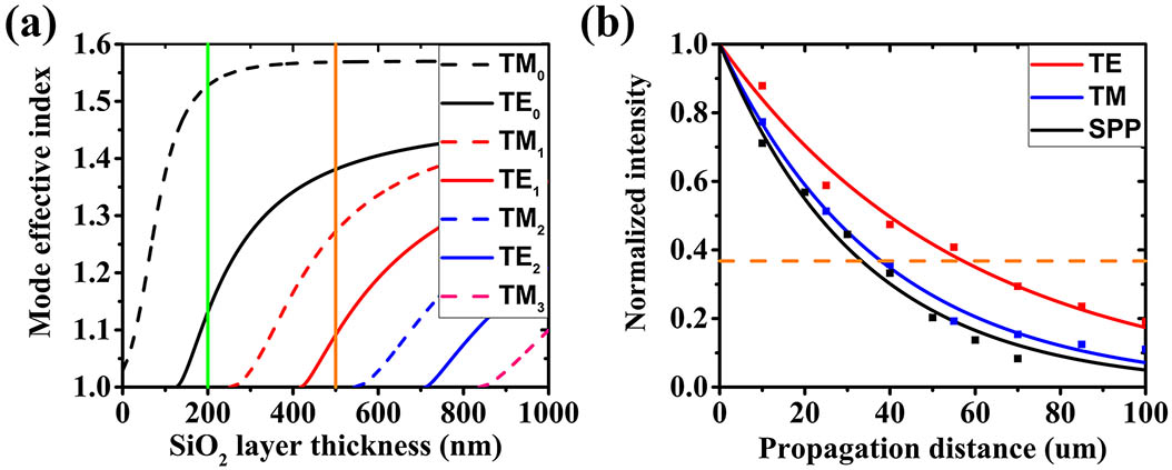
Fig. 1. (a) Calculated mode effective index of the DLPW with respect to different SiO2 layer thickness including all TE and TM modes. (b) The normalized loss measurement of SPP, TE, and TM modes. The symbols are the experimental data and the curves are the exponential fittings. The orange horizontal dotted line means the guided wave’s intensity attenuated to 1/e.

下载图片 查看所有图片

The experimental setup is shown in Fig. 2(a). Figure 2(b) shows the design of the DLPW. The guided modes are launched from a focused He–Ne laser (λ0=633nm) by a coupling grating and then propagate into well-arranged nanoscatterers. SiO2 (refractive index of n=1.46 at λ0=633nm) is chosen as the dielectric layer. Figure 2(c) schematically shows the scanning electron microscope (SEM) image of a fabricated sample. In the experiment, the grating and nanoscatterers were fabricated by a focused ion beam (FIB, dual-beam FEI Helios 600i, 30 kV, 40 pA) milling on a 300 nm thickness silver film that has been deposited on a 0.5 mm thickness quartz substrate. By carefully optimizing the experimental results, suitable structural parameters of the nanoscatterers were determined. All the rectangular-hole nanoscatterers were 300 nm in length, 100 nm in width, and 80 nm in depth. The orientations of the nanoscatterers were with a uniform 45° as shown in the zoom-in SEM image in Fig. 2(c), and can rotate the polarization of the scattered image to 45° to filter out the background noise to some extent in imaging measurement. Afterward, SiO2 was deposited by plasma enhanced chemical vapor deposition (PECVD, Oxford Plasmalab 80 Plus, 300°C) on the silver film.
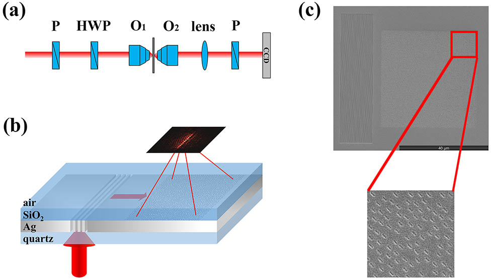
Fig. 2. (a) Illustration of the experimental setup; (b) a schematic of the DLPW where multiple modes are launched by a grating in the silver film from an incident laser beam and image over our sample; (c) a top-view scanning electron microscope (SEM) image of the couple-in grating and nanoscatterers in which the inset figure is the zoom-in image showing the details of the hologram units.

下载图片 查看所有图片

According to the MDM method introduced above, the designed object imaging could be reconstructed by a proper guided wave illumination on a well-arranged nanoscatterers hologram. It is necessary to mention that holography has a broadband effect that might lead to crosstalk when we use different modes for multiplexing. Fortunately, such a reconstruction cannot be totally fulfilled by other guided modes for their unsatisfied phase evolutions. Here, taking the focusing case and a 200 nm thickness single-mode waveguide for example, the effective mode indices of TM0 and TE0 are 1.53 and 1.13, respectively. The designed hologram is obtained by the interference of a spherical wave from a point source (z=25μm) and a TM0 mode propagating along the +x direction (30μm×30μm in size) as shown in Fig. 3(a), which means a reference TM0 mode propagating in the +x direction in the reconstruction process. When we excite the TM0 in the +x direction, a free-space spherical wave can be reconstructed by guided-mode scattering, which rightly gives rise to a focusing spot, as shown in Fig. 1(b). However, if we excite the TE0 [shown in Fig. 3(c)], the scattered wave will focus on a deformed spot with a large location shift, and its intensity is much lower than (only about 20%) that of the TM0 mode [shown in Fig. 3(d)]. Therefore, this crosstalk should be very weak and does not influence the demultiplexed holographic imaging. On this basis, we could possibly find a way to record multiple objects into a single hologram structure on a DLPW by using different guided-mode illuminations.
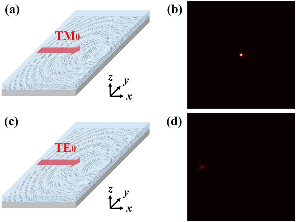
Fig. 3. Schematic of the guided-mode propagating through a well-designed hologram for (a) TM0 and (c) TE0 along the +x direction; (b) and (d) are the calculation results by the diffraction Huygens–Fresnel principle with respect to the hologram structures under TM0 and TE0 illumination, respectively. The size is 30μm×30μm.

下载图片 查看所有图片

For a good MDMH, a suitable design of the nanoscatterers distribution is important. Figures 4(a) and 4(b) show the 30μm×30μm hologram pattern of a single object letter ‘E’ with respect to the TE0 mode as the reference wave and letter ‘M’ with respect to the TM0 mode as the reference wave, respectively. The overlapped hologram pattern for two holographic images is shown in Fig. 4(c) and the zoom-in figure is presented in Fig. 4(d). The reference waves are both propagating along the +x direction, so the phase curvatures are in similar profiles, which makes them have less crossings [shown in Fig. 4(e)]. Here, there are only about hundreds of crossings between the two hologram profiles, which are not enough to reconstruct the multiplexed images. Then we select points from TE0’s hologram and TE1’s hologram to cover the entire sample randomly and one by one, which can guarantee that the ratio of them is 11. After that, the number of nanoscatterers is extended to about 3000. The final designed hologram structure with a well-selected nanoscatterers array is shown in Fig. 4(f).
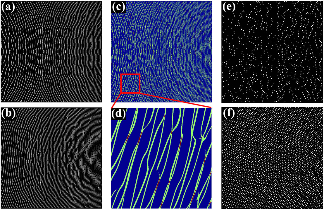
Fig. 4. (a) and (b) The 30μm×30μm hologram patterns of a single object letter ‘E’ with respect to the TE0 mode as the reference wave and letter ‘M’ with respect to the TM0 mode as the reference wave, respectively; (c) the overlapped hologram pattern for two holographic images, and (d) the zoom-in figure; (e) shared scatterers between two hologram patterns; (f) the final designed hologram structure with a well-selected nanoscatterers array.

下载图片 查看所有图片

Due to the different losses and polarizations of TM and TE modes, two kinds of MDM holography are carried out in experiments. One is the TM/TE-based MDMH, in which the guided modes can be launched by the same grating (according to a certain bandwidth) coupling by different polarization incidences. The sample was fabricated by FIB etching on silver film with PECVD depositing a 200 nm thick SiO2 to guarantee the lowest TE mode (TE0) supported. When a vertically polarized laser is incident on the grating of sample, the TE0 mode will be excited and propagate into the well-designed nanoscatterer hologram [shown in Fig. 5(a)]. When the polarization of the incident laser turns to horizontal, the coupled mode will change to TM0 [shown in Fig. 5(c)]. Since the TM mode has a larger loss, this hologram sample was designed in a size of 30μm×30μm, identical to the previous SPP case[34]. To demonstrate this approach, a multiplexed hologram encoding phase information on 10μm×10μm capital letters ‘E’ and ‘M’ is designed. Figures 5(b) and 5(d) show the experimental results of the demultiplexed holographic images at an image plane at 25 μm distance. Although there is some background noise, two holographic images composed of a series of points can be clearly observed with almost no crosstalk.
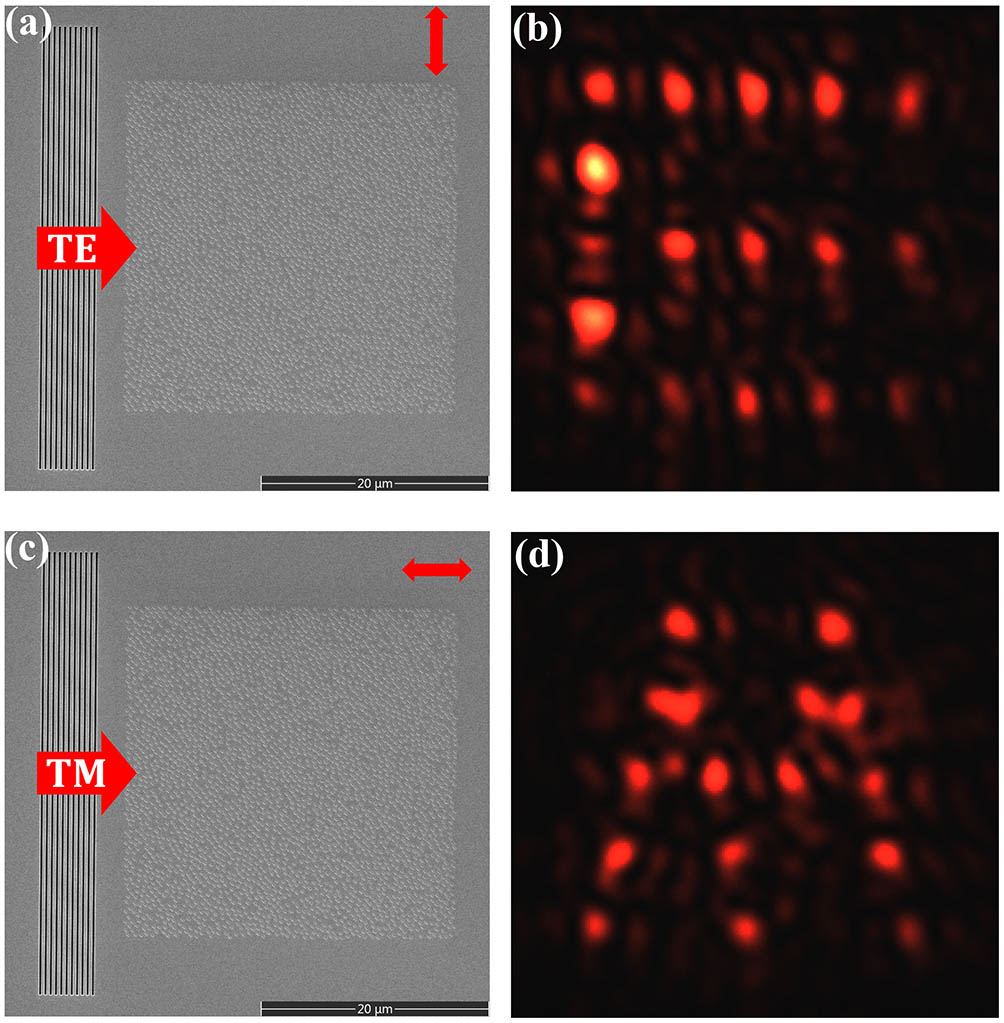
Fig. 5. (a) and (c) The SEM images of a couple-in grating and a multiplexed hologram by TE0 and TM0. The size of the nanoscatterers array is 30μm×30μm due to the loss of TM mode. The red arrow in the upper-right corner represents the polarization of the incident lights and the red arrow in the center-left with the letters ‘TE’ or ‘TM’ represents the excited guided mode. (b) and (d) The experimental measurements of the capital letters ‘E’ and ‘M’ images decoded from the multiplexed hologram according to TE and TM mode excitation, respectively.

下载图片 查看所有图片

The other approach is to multiplex multimodes in the same polarization and take the TE0/TE1-based MDMH as an example. The SiO2 thickness is chosen to be 500 nm to support both TE0 and TE1, whose effective refractive indices are 1.38 and 1.09, respectively. In the experiments, to exactly excite these two modes, two gratings with a large number of slits (41 in total) with different grating constants were used to launch the TE0 and TE1 modes according to their different wavenumbers, as shown in Figs. 6(a) and 6(c), respectively. Owing to the lower loss of TE modes, the hologram sample is designed in an expanded size of 60μm×60μm, and the size of the holographic images are also expanded twice as before at the imaging plane of 50 μm distance. The experimental results of the number ‘0’ image reconstructed by TE0 single mode excitement and the number ‘1’ image reconstructed by the TE1 single-mode excitement are vividly shown in Figs. 6(b) and 6(d), respectively. From the figures, two images can be clearly distinguished and almost no crosstalk in despite of some background noise, which indicates that the higher-ordered MDMH is successful. It is difficult to make an accurate analysis of the whole device efficiency due to the complex processes of guided-mode coupling, propagation, and scattering. To give a rough estimation according to our experimental data, the total efficiency would be approximately 2%–3%, and it can be further improved by optimizing the coupling and scattering processes. Nevertheless, what should be mainly emphasized here is this newly proposed MDM holographic design.
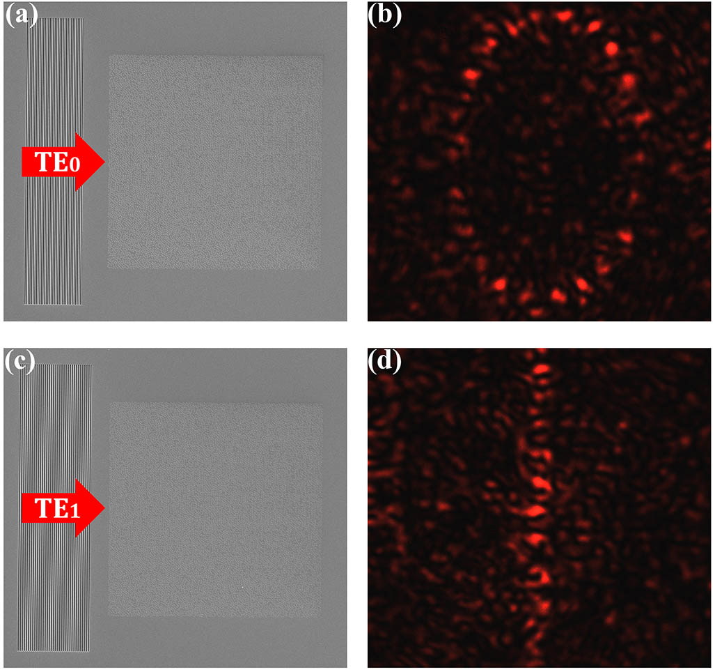
Fig. 6. (a) and (c) The SEM images of the totally same multiplexed hologram by TE0 and TE1 but different couple-in gratings with different periods. The size of the nanoscatterers arrays is 60μm×60μm due to the low loss of the TE mode. The periods of the gratings in (a) and (c) are equal to the effective wavelengths of TE0 and TE1, respectively. (b) and (d) The experimental measurements of the number ‘0’ and ‘1’ images decoded from the multiplexed hologram according to TE0 and TE1 mode excitation, respectively.

下载图片 查看所有图片

In conclusion, we theoretically proposed and experimentally demonstrated mode division multiplexed holograms based on DLPW. Both TM/TE and TE0/TE1 multiplexed holograms were successfully obtained with almost no crosstalk. Thanks to the low-loss property of the TE mode, a much larger hologram pattern of 60μm×60μm size is presented, which indicates the possibility of upsizing the scale of such kinds of on-chip holographic devices, and can even be thoroughly extended to the all-dielectric waveguide systems. Although there is still some background noise, we believe it could be further optimized, and the multiplexing capability can be further upgraded by incorporating with the previous multiplexing in propagation directions and scattering polarizations.

References

[1] GaborD., Nature161, 777 (1948).

[2] BrownB. R.LohmannA. W., Appl. Opt.5, 967 (1966).APOPAI0003-6935

[3] YuN.GenevetP.KatsM. A.AietaF.TetienneJ.-P.CapassoF.GaburroZ., Science334, 333 (2011).SCIEAS0036-8075

[4] HuangL.ChenX.MühlenberndH.LiG.BaiB.TanQ.JinG.ZentgrafT.ZhangS., Nano Lett.12, 5750 (2012).NALEFD1530-6984

[5] SunS.HeQ.XiaoS.XuQ.LiX.ZhouL., Nat. Mater.11, 426 (2012).NMAACR1476-1122

[6] KildishevA. V.BoltassevaA.ShalaevV. M., Science339, 1232009 (2013).SCIEAS0036-8075

[7] YinX.YeZ.RhoJ.WangY.ZhangX., Science339, 1405 (2013).SCIEAS0036-8075

[8] KarimiE.SchulzS. A.De LeonI.QassimH.UphamJ.BoydR. W., Light Sci. Appl.3, e167 (2014).

[9] MontelongoY.Tenorio-PearlJ. O.WilliamsC.ZhangS.MilneW. I.WilkinsonT. D., Proc. Natl. Acad. Sci.111, 12679 (2014).

[10] ArbabiA.HorieY.BagheriM.FaraonA., Nat. Nanotechnol.10, 937 (2015).NNAABX1748-3387

[11] ChenX.HuangL.MühlenberndH.LiG.BaiB.TanQ.JinG.QiuC.-W.ZhangS.ZentgrafT., Nat. Commun.3, 1198 (2012).NCAOBW2041-1723

[12] YeW.ZeunerF.LiX.ReinekeB.HeS.QiuC.-W.LiuJ.WangY.ZhangS.ZentgrafT., Nat. Commun.7, 11930 (2016).NCAOBW2041-1723

[13] ChenW. T.YangK.-Y.WangC.-M.HuangY.-W.SunG.ChiangI. D.LiaoC. Y.HsuW.-L.LinH. T.SunS.ZhouL.LiuA. Q.TsaiD. P., Nano Lett.14, 225 (2014).NALEFD1530-6984

[14] DuJ.WangJ., Opt. Express26, 13183 (2018).OPEXFF1094-4087

[15] ZhaoY.DuJ.ZhangJ.ShenL.WangJ., Appl. Phys. Lett.112, 171103 (2018).APPLAB0003-6951

[16] WangJ., Chin. Opt. Lett.16, 050006 (2018).CJOEE31671-7694

[17] NiX.KildishevA. V.ShalaevV. M., Nat. Commun.4, 2807 (2013).NCAOBW2041-1723

[18] HuangL.ChenX.MühlenberndH.ZhangH.ChenS.BaiB.TanQ.JinG.CheahK.-W.QiuC.-W.LiJ.ZentgrafT.ZhangS., Nat. Commun.4, 2808 (2013).NCAOBW2041-1723

[19] ZhengG.MühlenberndH.KenneyM.LiG.ZentgrafT.ZhangS., Nat. Nanotechnol.10, 308 (2015).NNAABX1748-3387

[20] WenD.YueF.LiG.ZhengG.ChanK.ChenS.ChenM.LiK. F.WongP. W. H.CheahK. W.Y. B. PunE.ZhangS.ChenX., Nat. Commun.6, 8241 (2015).NCAOBW2041-1723

[21] MalekS. C.EeH.-S.AgarwalR., Nano Lett.17, 3641 (2017).NALEFD1530-6984

[22] WangJ.ZhangJ.WuX.LuoH.GongQ., Appl. Phys. Lett.94, 081116 (2009).APPLAB0003-6951

[23] GonzálezM. U.WeeberJ. C.BaudrionA. L.DereuxA.StepanovA. L.KrennJ. R.DevauxE.EbbesenT. W., Phys. Rev. B73, 155416 (2006).

[24] SiviloglouG. A.BrokyJ.DogariuA.ChristodoulidesD. N., Phys. Rev. Lett.99, 213901 (2007).PRLTAO0031-9007

[25] EllenbogenT.Voloch-BlochN.Ganany-PadowiczA.ArieA., Nat. Photon.3, 395 (2009).NPAHBY1749-4885

[26] LiL.LiT.WangS. M.ZhangC.ZhuS. N., Phys. Rev. Lett.107, 126804 (2011).PRLTAO0031-9007

[27] LiL.LiT.WangS.ZhuS.ZhangX., Nano Lett.11, 4357 (2011).NALEFD1530-6984

[28] ZhangP.HuY.LiT.CannanD.YinX.MorandottiR.ChenZ.ZhangX., Phys. Rev. Lett.109, 193901 (2012).PRLTAO0031-9007

[29] LiL.LiT.WangS. M.ZhuS. N., Phys. Rev. Lett.110, 046807 (2013).PRLTAO0031-9007

[30] ChenJ.LiL.LiT.ZhuS. N., Sci. Rep.6, 28926 (2016).SRCEC32045-2322

[31] LiL.LiT.TangX.-M.WangS.-M.WangQ.-J.ZhuS.-N., Light Sci. Appl.4, e330 (2015).

[32] OzakiM.KatoJ.-i.KawataS., Science332, 218 (2011).SCIEAS0036-8075

[33] DolevI.EpsteinI.ArieA., Phys. Rev. Lett.109, 203903 (2012).PRLTAO0031-9007

[34] ChenJ.LiT.WangS.ZhuS., Nano Lett.17, 5051 (2017).NALEFD1530-6984

[35] ChengQ. Q.LiT.LiL.WangS. M.ZhuS. N., Opt. Lett.39, 3900 (2014).OPLEDP0146-9592

[36] ChengQ. Q.LiT.GuoR. Y.LiL.WangS. M.ZhuS. N., Appl. Phys. Lett.101, 171116 (2012).APPLAB0003-6951

[37] LiL.LiT.WangS. M.ZhuS. N., Opt. Lett.37, 5091 (2012).OPLEDP0146-9592

[38] TangX. M.LiL.LiT.WangQ. J.ZhangX. J.ZhuS. N.ZhuY. Y., Opt. Lett.38, 1733 (2013).OPLEDP0146-9592

Chenchen Zhao, Ji Chen, Hanmeng Li, Tao Li, Shining Zhu. Mode division multiplexed holography by out-of-plane scattering of plasmon/guided modes[J]. Chinese Optics Letters, 2018, 16(7): 070901.

引用该论文: TXT   |   EndNote

相关论文

加载中...

关于本站 Cookie 的使用提示

中国光学期刊网使用基于 cookie 的技术来更好地为您提供各项服务,点击此处了解我们的隐私策略。 如您需继续使用本网站,请您授权我们使用本地 cookie 来保存部分信息。
全站搜索
您最值得信赖的光电行业旗舰网络服务平台!