Chinese Optics Letters, 2020, 18 (1): 012501, Published Online: Dec. 30, 2019
Bias-free operational monolithic symmetric-connected photodiode array  Download: 783次
Figures & Tables
Fig. 1. (a) Capacitance-voltage characteristics of the UTC-PD with different doping concentrations in the collection layer. (b) The electric field distribution of the UTC-PD with the different doping concentrations in the collection layer under zero bias.
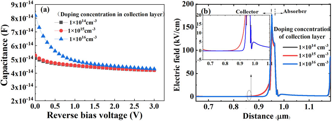
Fig. 2. Schematic experiment setup of the (a) frequency response and (b) RF output power. The inserted figure is the micrograph of the fabricated SC-PDA with 15 μm diameter of each PD.

Fig. 3. (a) Measured dark current of the SC-PDA versus the PD diameter. (b) Measured DC response of the fabricated SC-PDA, the SC-PDA in Ref. [12], and the corresponding single PD element. The data were measured with 1550 nm incident light without bias.

Fig. 4. Measured frequency response of the fabricated SC-PDA with the 15 μm diameter PD elements at 500 μA photocurrent.

Fig. 5. Measured 3 dB bandwidth versus different diameters of the PD elements under zero bias at 1 mA photocurrent.

Fig. 6. Measured capacitance of the fabricated SC-PDA and the corresponding single PD element with different diameters without bias at 1 mA photocurrent. The inserted figure is the capacitance versus different diameter of the PD when the RF frequency is 10 GHz.

Fig. 7. Measured small signal frequency response of the SC-PDA and PD elements with a diameter of 50 μm at 0 V bias and a photocurrent of 2 mA.


Table1. Epitaxial Structure of the UTC-PD
|
Dan Yang, Yongqing Huang, Tao Liu, Xiaokai Ma, Xiaofeng Duan, Kai Liu, Xiaomin Ren. Bias-free operational monolithic symmetric-connected photodiode array[J]. Chinese Optics Letters, 2020, 18(1): 012501.


 PDF全文
PDF全文

